


HD49335NP/HNP
Rev.1.0, Feb.12.2004, page 16 of 29
Electrical Characteristics (cont.)
(Unless othewide specified, Ta = 25°C, AV
DD
= 3.0 V, DV
DD
= 3.0 V, and R
BIAS
= 33 kΩ)
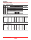
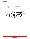
• Items for ADCIN Input Mode
Item Symbol Min Typ Max Unit Test Conditions Remarks
Consumption current (3) I
DD3
— 32 38.4 mA f
CLK
= 36 MHz
ADCIN mode
LoPwr = low
Consumption current (4) I
DD4
— 22 27.5 mA f
CLK
= 25 MHz
ADCIN mode
LoPwr = high
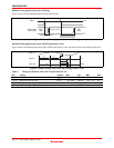
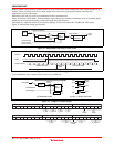
Timing specifications (14) t
ADC1
— (6) — ns
Timing specifications (15) t
ADC2
Typ × 0.85 1/2f
ADCLK
Typ × 1.15 ns
Timing specifications (16) t
ADC3
Typ × 0.85 1/2f
ADCLK
Typ × 1.15 ns
Timing specifications (17) t
AHLD4
— (14.5) — ns C
L
= 10 pF
Timing specifications (18) t
AOD5
— (23.5) — ns C
L
= 10 pF
Refer to table 9
Input current at ADC input IIN
CIN
–110 — 110 µA V
IN
= 1.0 to 2.0 V
Clamp level at ADC input OF2 — (512) — LSB
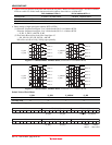
GSL(0) 0.45 0.57 0.72 Times
GSL(63) 1.36 1.71 2.16 Times
GSL(127) 2.27 2.86 3.60 Times
GSL(191) 3.18 4.00 5.04 Times
PGA gain at ADC input
GSL(255) 4.08 5.14 6.47 Times
Note : Values within parentheses ( ) are for reference.