HD49335NP/HNP
Rev.1.0, Feb.12.2004, page 14 of 29
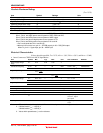
Absolute Maximum Ratings
(Ta = 25°C)
Item Symbol Ratings Unit
Power supply voltage V
DD
4.1 V
Analog input voltage V
IN
–0.3 to AV
DD
+0.3 V
Digital input voltage V
I
–0.3 to DV
DD
+0.3 V
Operating temperature range Ta –10 to +75 °C
Power dissipation Pt 750 mW
Storage temperature Tstg –55 to +125 °C
Power supply voltage Vopr 2.70 to 3.30 V
Note: AV
DD
, AV
SS
are analog power source systems of CDS, PGA, and ADC.
DV
DD
1, DV
SS
1 are digital power source systems of CDS, PGA and ADC.
DV
DD
2, DV
SS
2 are buffer power source systems of ADC output.
DV
DD
3, DV
SS
3 are general digital power source systems of TG.
DV
DD
4, DV
SS
4 are buffer power source systems of H1 and H2.
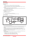
• Pin 2 multi bonds the DV
SS
1 and DV
SS
2
• When pin 64 is set to Low, pin 41 = STROB output, pin 39 = SUB_SW output
When Hi, pin 41 = Vgate input, pin 39 = ADCK input
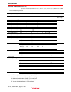
Electrical Characteristics
(Unless othewide specified, Ta = 25°C, AV
DD
= 3.0 V, DV
DD
= 3.0 V, and R
BIAS
= 33 kΩ)
• Items Common to CDSIN and ADCIN Input Modes
Item Symbol Min Typ Max Unit Test Conditions Remarks
Power supply voltage
range
V
DD
2.70 3.00 3.30 V
f
CLK
hi 20 — 36 MHz LoPwr = low *
2
HD49335HNP Conversion frequency
f
CLK
low 5.5 — 25 MHz LoPwr = high *
2
HD49335NP
V
IH2
DV
DD
3.0
2.25 ×
— DV
DD
V
Digital input voltage
V
IL2
0 —
DV
DD
3.0
0.6 ×
V
CS, SCK, SDATA
V
OH
DV
DD
–0.5 — — V I
OH
= –1 mA Digital output voltage
V
OL
— — 0.5 V I
OL
= +1 mA
I
IH
— — 50 µA V
IH
= 3.0 V Digital input current
I
IL
–50 — — µA V
IL
= 0 V
ADC resolution RES 10 10 10 bit
ADC integral linearity INL — (2) — LSBp-p f
CLK
= 25 MHz
ADC differential linearity+ DNL+ — 0.3 0.99 LSB f
CLK
= 25 MHz *1
ADC differential linearity– DNL– –0.99 –0.3 — LSB f
CLK
= 25 MHz *1
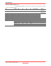
Sleep current I
SLP
–100 0 100 µA
Digital input pin is
set to 0 V, output
pin is open
Standby current I
STBY
— 3 5 mA
Digital I/O pin is set
to 0 V
Notes: 1. Differential linearity is the calculated difference in linearity errors between adjacent codes.
2. 2 divided mode: f
CLK
= 1/2CLK_in
3 divided mode: f
CLK
= 1/3CLK_in
3. Values within parentheses ( ) are for reference.


