HD49335NP/HNP
Rev.1.0, Feb.12.2004, page 26 of 29
Notice for Use
1. Careful handling is necessary to prevent damage due to static electricity.
2. This product has been developed for consumer applications, and should not be used in non-consumer applications.
3. As this IC is sensitive to power line noise, the ground impedance should be kept as small as possible. Also, to
prevent latchup, a ceramic capacitor of 0.1 µF or more and an electrolytic capacitor of 10 µF or more should be
inserted between the ground and power supply.
4. Common connection of AV
DD
and DV
DD
should be made off-chip. If AV
DD
and DV
DD
are isolated by a noise filter,
the phase difference should be 0.3 V or less at power-on and 0.1 V or less during operation.
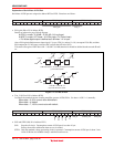
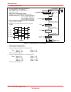
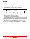
5. If a noise filter is necessary, make a common connection after passage through the filter, as shown in the figure
below.
HD49335
AV
SS
DV
SS
AV
DD
DV
DD
1 to 4
Noise filter
A
nalog
+3.0V
HD49335
DV
SS
AV
SS
DV
DD
1 to 4 AV
DD
100 µH
0.01 µF
Noise filter Example of noise filte
r
Digital
+3.0V
0.01 µF
6. Connect AV
SS
and DV
SS
off-chip using a common ground. If there are separate analog system and digital system
set grounds, connect to the analog system.
7. When V
DD
is specified in the data sheet, this indicates AV
DD
and DV
DD
.
8. No Connection (NC) pins are not connected inside the IC, but it is recommended that they be connected to power
supply or ground pins or left open to prevent crosstalk in adjacent analog pins.
9. To ensure low thermal resistance of the package, a Cu-type lead material is used. As this material is less tolerant of
bending than Fe-type lead material, careful handling is necessary.
10. The infrared reflow soldering method should be used to mount the chip. Note that general heating methods such as
solder dipping cannot be used.
11. Serial communication should not be performed during the effective video period, since this will result in degraded
picture quality. Also, use of dedicated ports is recommended for the SCK and SDATA signals used in the
HD49330AF. If ports are to be shared with another IC, picture quality should first be thoroughly checked.
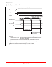
12. At power-on, automatic adjustment of the offset voltage generated from PGA, ADC, etc., must be implemented in
accordance with the power-on operating sequence (see page 24).
13. Ripple noise of DC/DC converter which generates the voltage of analog part should set under –50 dB with power
supply voltage.


