HD49335NP/HNP
Rev.1.0, Feb.12.2004, page 21 of 29
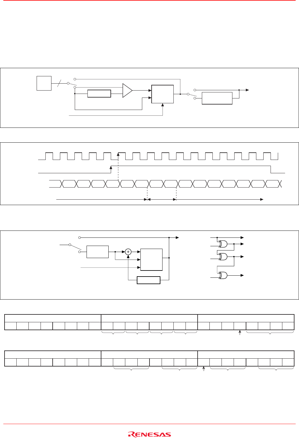
Ripple (pseudo outline made by quantized error) occurres on the point which swithing the ADC output multiple bit in
parallel. When switching the several of ADC output at the same time, ripple (pseudo outline caused by miss
quantization) occurs to the image.
Differential code and gray code are recommended for this countermeasure.
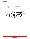
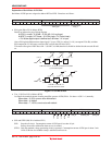
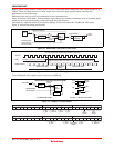
Figure 10 indicates circuit block. When luminance signal changes are smoothly, the number of bit of switching digital
output bit can be reduced and easily to reduce the ripple using this function.
This function is especially effective for longer the settings of sensor more than clk = 30 kHz, and ADC output.
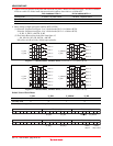
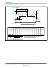
Figure 11 indicates the timing specifications.
ADC
10
Differential SW(D9)
Carry bit
round
+
−
Gray SW(D8)
Standard data
control signal
(D12,D11,D10)
Standard
data
selector
10-bit
output
2clk_DL
Gray→Binary
conversion
Figure 10 Differential Code, Gray Code Circuit
1
A
DCLK
OBP
Digital output
(Beginning edge of OBP and standard edge of ADCLK should be exept ±5 ns)
(In case of select the positive edge of ADCLK with D12)
(In case of select the positive polar)
Differential data Standard
data
Differential data
234567891011
Figure 11 Differential Code Timing Specifications
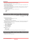
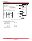
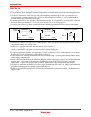
To use differential code, complex circuit is necessary at DSP side.
(1) Differential coded
From ADC
Standard data
control signal
Carry bit
round
2clk_DL
Standard
data
selector
D11 D11
D10
D9
D0
D10
D9
D0
Gray →
Binary
(2) Gray → Binary conversion
Figure 12 Complex Circuit Example
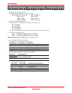
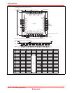
Address STD1[7:0] (L) STD2[15:8] (H)
11110101 D4D3D2D7 D6 D5 D1 D0 D12 D11 D10 D9 D8
P_SP1P_SP2P_ADCLKP_RG DLL
steps
DLL
current
2,3 divided
select
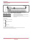
Address STD1[7:0] (L) STD2[15:8] (H)
11111000 D4 D2D6 D5 D1 D0 D12 D10D15 D14 D13 D9 D8
P_SP2 P_SP1 P_ADCLKP_RG


