HD49335NP/HNP
Rev.1.0, Feb.12.2004, page 17 of 29
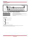
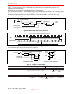
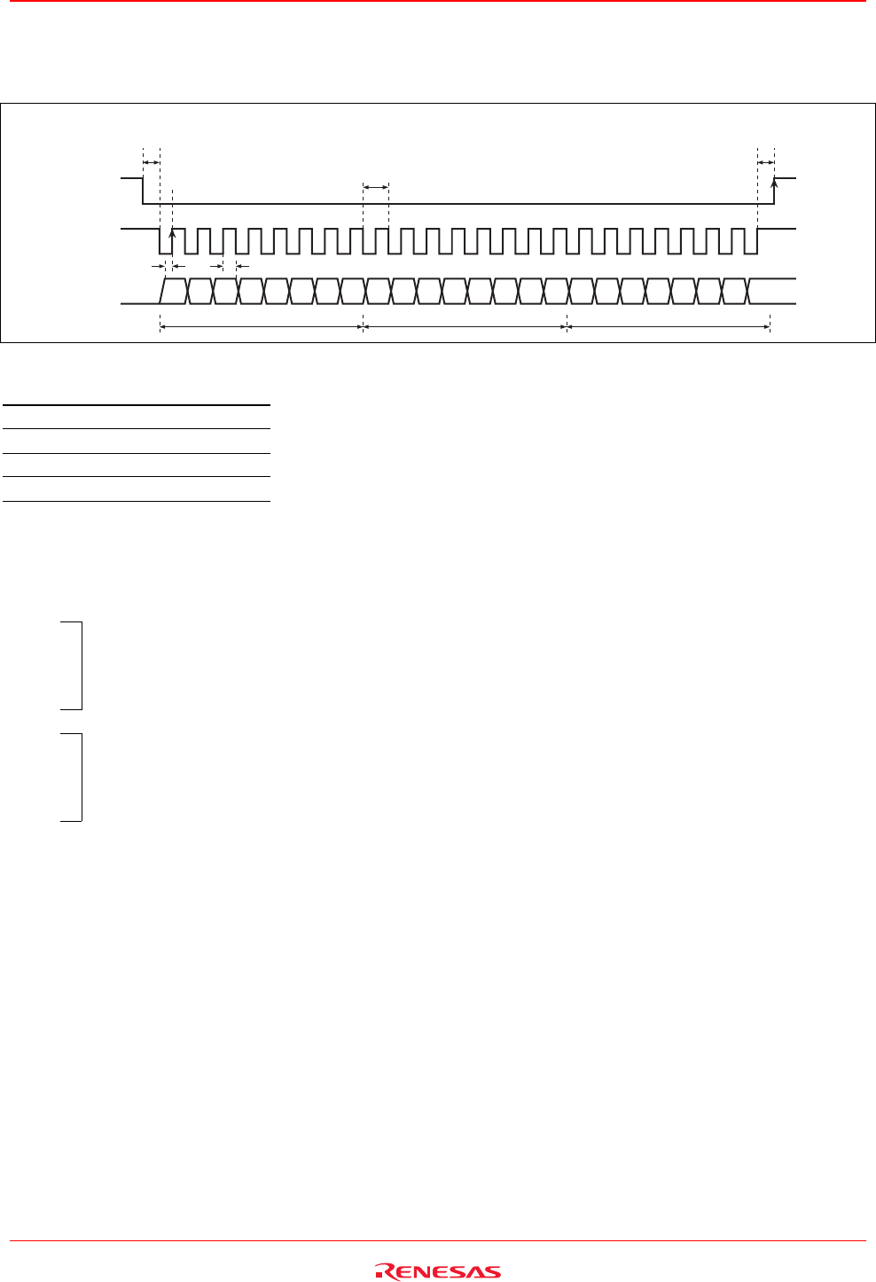
Serial Interface Specifications
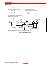
Timing Specifications
SDATA
STD2(Upper data) STD1(Lower data) address(address)
SCK
CS
f
SCK
D9D8 D11D10 D13D12 D15D14 D1D0 D3D2 D5D4 D7D6 D0 D2D1 D4D3 D6D5 D7
t
INT1
t
INT2
t
su
t
ho
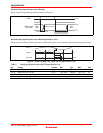
Latches SDATA
at SCK rising edge
Data is determined
at CS rising edge
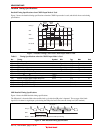
Figure 8 Serial Interface Timing Specifications
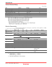
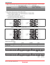
Item Min Max
f
SCK
— 5 MHz
t
INT1,2
50 ns —
t
su
50 ns —
t
ho
50 ns —
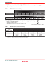
Notes: 1. 3 byte continuous communications.
2. Input SCK with 24 clock when CS is Low.
3. It becomes invalid when data communications are stopped on the way.
4. Data becomes a default with hardware reset.
5. Input more than double frequency of SCK to the CLK_in when transfer
the serial data.
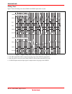
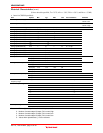
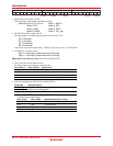
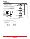
The Kind of Data
Data address has 256 type. H’00 to H’FF
H’00
:
:
H’EF
Data at timing generator part
H’F0
:
:
H’FF
Data at CDS part
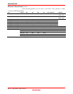
Address map of each data referred to other sheet.
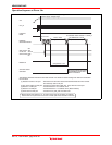
Details of timing generator refer to the timing chart on the other sheet together with this specification.
This specification only explains about the data of CDS part.


