HD49335NP/HNP
Rev.1.0, Feb.12.2004, page 19 of 29
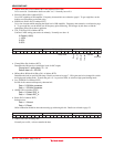
• Output mode (D2 to D4 of address H’F1 and address H’F4 of D6)
It is a test mode. Combination details are table 3 to 5. Normally set to all 0.
• SHA-fsel (D8 to D9 of address H’F1)
It is a LPF switching of SH amplifier. Frequency characteristics are referred to page 8. To get rough idea, set the
double cut off frequency point with using.
• SHSW-fsel (D10 to D13 of address H’F1)
It is a time constant which sampling the black level of SH amplifier. Frequency characteristics are referred to page
8. To get rough idea, set the double cut off frequency point with using. S/N changes by this data, so find the
appropriate point with set data to up/down.
• Test_I2 (D14 to D15 of address H’F1)
Current of ADC analog part can be set minutely. Normally use data = 0.
0: Default (100%)
1: 150%
2: 50%
3: 80%
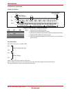
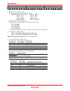
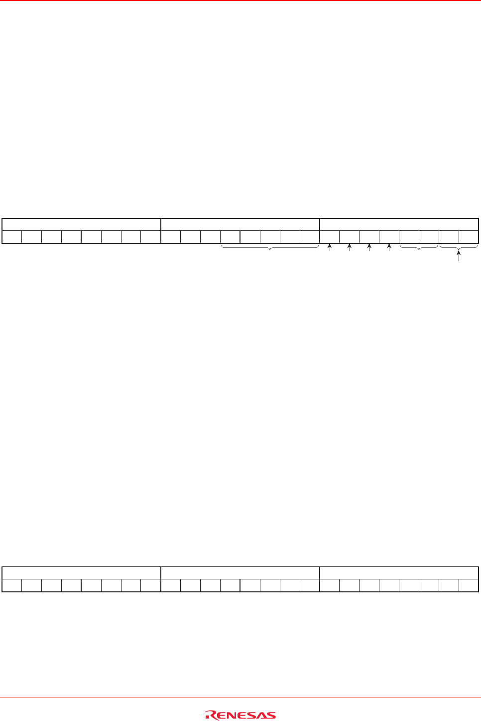
Address STD1[7:0] (L)
HGain-Nsel
STD2[15:8] (H)
1 1 1 1 0 0 1 0 D4 D3 D2 D1 D0 D15 D14 D13 D12 D11 D10 D9
D8
Clamp level
Reset
AD_sel
CDS_buff
Low_pwr
HGstop-Hsel
• Clamp (D0 to D4 of address H’F2)
Determine the OB part level with digital code of ADC output.
Clamp level = setting data × 2 + 14
Default data is 9 = 32 LSB.
• HGstop-Hsel, HGain-Nsel (D8 to D11 of address H’F2)
Determine the lead-in speed of OB clamp. Details are referred to page 7. PGA gain need to be changed for switch
the high speed leading mode. Transfer the gain +1/–1 to previous field, its switch to high speed leading mode.
• Low_PWR (D12 of address H’F2)
Switch circuit current and frequency characteristic.
Data = 0: 36 MHz guarantee
Data = 1: 25 MHz guarantee
• ADSEL (D14 of address H’F2)
Data = 0: Select CDS_in
Data = 1: Select ADC_in
• Reset (D15 of address H’F2)
Software reset.
Data = 1: Normal
Data = 0: Reset
Offset calibration should be done when starting up with using this bit. Details are referred to page 23.
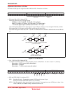
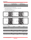
Address STD1[7:0] (L) STD2[15:8] (H)
11110011 D4D3D2D7 D6 D5 D1 D0 D15 D14 D13 D12 D11 D10 D9 D8
• Address H'F3 are all testing data.
Normally set to all 0., or do not transfer the data.


