


( 31 / 42 )
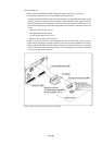
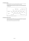
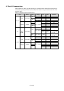
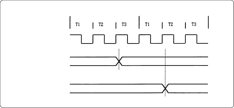
Figure 5.2 P0, P1 and D port output timings
5.6 Port I/O Timing
(1) Port input timing
Port input timings are the same as with the actual MCUs.
(2) Port output timing
When using the M34514T-MCU, output timings are different from those of the actual MCUs for
the following ports that are configured with port emulation circuits:
• Ports P00 to P03
• Ports P10 to P13
• Ports D0 to D5
With the actual MCUs, changes occur at the beginning of the T3 state of an output instruction.
With the M34514T-MCU, changes occur at the beginning of the T2 state of the next output
instruction. Figure 5.2 shows the port output timings of the actual MCUs and M34514T-MCU.
For the other ports, the output timings are the same as with the actual MCUs.
Next output instructionOutput instruction
System clock
X
IN
P0, P1, D port
output timings
on actual MCUs
P0, P1, D port
output timings of
M34514T-MCU