


DISK DRIVE OPERATION
SpinPoint V40 Product Manual
40
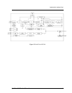
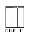
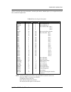
6.2.3 Signal Descriptions
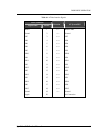
The interface signals and pins are described below and listed in Table 6-1. The signals are listed according to
function, rather than in numerical connector pin order.
6.2.3.1 CS1FX- (Drive Chip Select 0)
This is the chip select signal decoded from the host address bus used to select the Command Block registers.
6.2.3.2 CS3FX- (Drive Chip Select 1)
This is the chip select signal decoded from the host address bus used to select the Control Block registers.
6.2.3.3 DA0-2 (Drive Address Bus)
This is the 3-bit binary coded address asserted by the host to access a register or data port in the drive.
6.2.3.4 DASP- (Drive Active/Slave Present)
This is a time-multiplexed signal that indicates that a drive is active, or that Drive 1 is present. This signal is
an open collector output, and each drive has a 10K ohm pull-up resistor on this signal.
During power-on initialization or after RESET- is negated, DASP- is asserted by Drive 1 within 400 msec to
indicate that Drive 1 is present. Drive 0 allows up to 450 msec for Drive 1 to assert DASP-. If Drive 1 is not
present, Drive 0 may assert DASP- to drive an activity LED. DASP- is negated following acceptance of the
first valid command by Drive 1 or after 31 seconds, whichever comes first. Any time after negation of
DASP-, either drive may assert DASP- to indicate that a drive is active.
6.2.3.5 DD0-DD15 (Drive Data Bus)
This is an 8- or 16-bit bi-directional data bus between the host and the drive. The lower 8 bits are used for 8-
bit transfers (e.g., registers, ECC bytes).
6.2.3.6 DIOR- (Drive I/O Read)
This is the Read strobe signal. The falling edge of DIOR- enables data from a register or the data port of the
drive onto the host data bus, DD0-DD7 or DD0-DD15. The rising edge of DIOR- latches data at the host.
6.2.3.7 DIOW- (Drive I/O Write)
This is the Write strobe signal. The rising edge of DIOW- clocks data from the host data bus, DD0-DD7 or
DD0- DD15, into a register or the data port of the drive.