


vi SpinPoint V40 Product Manual
6.7.4 Ultra DMA data transfer ..........................................................................................................96
6.7.4.1 Initiating an Ultra DMA data in burst.................................................................................................. 96
6.7.4.2 Ultra DMA data burst timing requirements......................................................................................... 97
6.7.4.3 Sustained Ultra DMA data in burst...................................................................................................... 98
6.7.4.4 Host pausing an Ultra DMA data in burst ........................................................................................... 99
6.7.4.5 Device terminating an Ultra DMA data in burst................................................................................ 100
6.7.4.6 Host terminating an Ultra DMA data in burst....................................................................................101
6.7.4.7 Initiating an Ultra DMA data out burst.............................................................................................. 102
6.7.4.8 Sustained Ultra DMA data out burst..................................................................................................103
6.7.4.9 Device pausing an Ultra DMA data out burst.................................................................................... 104
6.7.4.10 Host terminating an Ultra DMA data out burst............................................................................. 105
6.7.4.11 Device terminating an Ultra DMA data out burst ......................................................................... 106
CHAPTER 7 MAINTENANCE.............................................................................................................107
7.1 G
ENERAL INFORMATION.................................................................................................................107
7.2 M
AINTENANCE PRECAUTIONS ........................................................................................................107
7.3 S
ERVICE AND REPAIR.....................................................................................................................107
TABLE OF TABLES
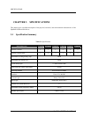
Table 3-1 Specifications............................................................................................................................6
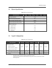
Table 3-2 Physical Specifications..............................................................................................................7
Table 3-3 Logical Configurations..............................................................................................................7
Table 3-4 Performance Specifications.......................................................................................................8
Table 3-5 Power Requirements .................................................................................................................9
Table 3-6 Environmental Specifications..................................................................................................10
Table 3-6 Environmental Specifications (continued)..............................................................................11
Table 3-7 Reliability Specifications ........................................................................................................11
Table 4-1 Power Connector Pin Assignment...........................................................................................16
Table 4-2 Logical Drive Parameters........................................................................................................21
Table 6-1 AT-Bus Interface Signals........................................................................................................43
Table 6-2 Interface Signals Description ..................................................................................................45
Table 6-3 I/O Port Function/Selection Address.......................................................................................48
Table 6-4 Command Codes and Parameters............................................................................................54
Table 6-5 Diagnostic Codes ....................................................................................................................57
Table 6-6 IDENTIFY DEVICE information...........................................................................................58
Table 6-7 Automatic Standby Timer Periods..........................................................................................62
Table 6-8 Set Feature Register Definitions..............................................................................................67
Table 6-9 Transfer mode values ..............................................................................................................67
Table 6-10 SMART Feature register values............................................................................................71
Table 6-11 Device SMART data structure..............................................................................................73
Table 6-12 Off-line data collection status values ....................................................................................74
Table 6-13 Command Errors...................................................................................................................80
Table 6-14 Power Saving Mode..............................................................................................................81
Table 6-15 Power Conditions..................................................................................................................82
Table 6-16 Register transfer to/from device............................................................................................91
Table 6-17 PIO data transfer to/from device ...........................................................................................93
Table 6-18 Multiword DMA data transfer...............................................................................................95
Table 6-19 Ultra DMA data burst timing requirements...........................................................................97