


Ethernet-DK
Rev. 0.6 31
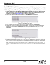
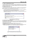
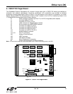
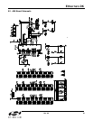
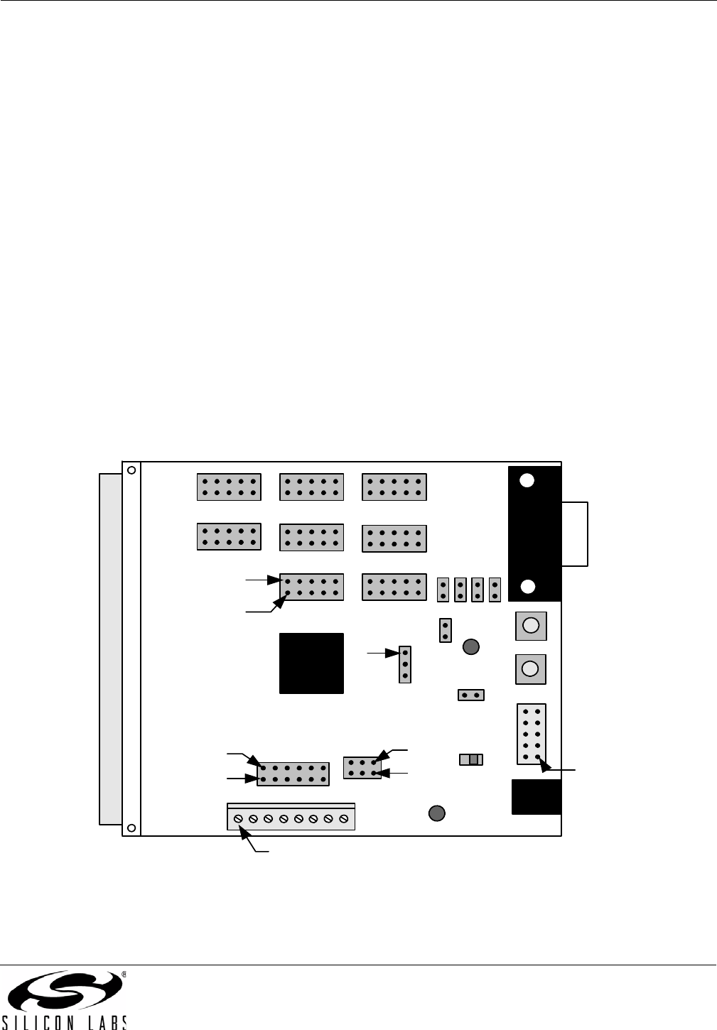
8. C8051F120 Target Board
The Embedded Ethernet Development Kit includes a target board with a C8051F120 device pre-installed for
evaluation and software development. Numerous input/output (I/O) connections are provided to facilitate
prototyping using the target board. Refer to Figure 27 for the locations of the various I/O connectors. For further
details, see the “C8051F12x Development Kit User’s Guide” located on the kit CD or installed by default in the
“C:\SiLabs\MCU\Documentation\Users Guides” directory.
P1 Power connector (accepts input from 7 to 15 VDC unregulated power adapter)
J1 Connects SW2 to P3.7 pin
J3 Connects LED D3 to P1.6 pin
J4 JTAG connector for Debug Adapter interface
J5 DB-9 connector for UART0 RS232 interface
J6 Connector for UART0 TX (P0.0)
J8 Connector for UART0 RTS (P4.0)
J9 Connector for UART0 RX (P0.1)
J10 Connector for UART0 CTS (P4.1)
J11 Analog loopback connector
J12–J19 Port 0–7 connectors
J20 Analog I/O terminal block
J22 VREF connector
J23 VDD Monitor Disable
J24 96-pin Expansion I/O connector
R1 Current Limiting Resistor For 96-pin Interface.
Note: R1 should be shorted with a zero ohm resistor if the 'F120TB is providing power to the AB4.
Figure 27. C8051F120 Target Board
C8051
F12X
J1
JTAG
RESET
P3.7
P1
J24
Pin 1
Pin 1
Pin 1
J11
Pin 2
J3
J23
PWR
P1.6
J5
J20
Pin 1
Pin 2
J22
Pin 2
Pin 1
Port 0 Port 2
Port 4
Port 7
Port 1
Port 3Port 6Port 5
J4
J9J6
J8J10
Pin 1
R1