


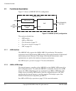
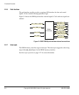
Functional Overview
2-10 Copyright © 2006 ARM Limited. All rights reserved. ARM DDI 0389B
Registered HWDATA
The interconnect used within the AHB MC contains combinatorial paths for the write
data. To improve the synthesis timing, HWDATA is registered and makes these paths
internal to the design.
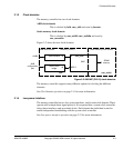
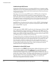
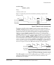
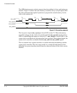
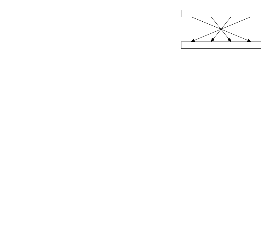
Big-endian 32-bit mode
The AHB MC supports the option of storing data to memory in big-endian 32-bit mode.
Each bridge contains the logic to implement this data mapping depending on the
big_endian input tie-off. Figure 2-5 shows that if the tie off is asserted then the data
buses are reordered.
Figure 2-5 Big-endian implementation
Removal of AHB error response logic
The internal protocol used within AHB MC supports the concept of errors. However
none of the components used ever generate errors. This means that the bridge does not
require any logic to generate AHB errors because there are no circumstances when
errors can be generated.
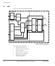
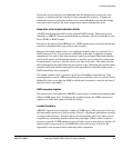
2.3.2 AHB to APB bridge operation
The internal memory controller has an APB configuration port. The AHB configuration
port is mapped to it using an AHB to APB bridge. Figure 2-6 on page 2-11 shows that
each internal memory controller configuration port has a 4KB address space.
%LJHQGLDQPRGH
/LWWOHHQGLDQGHIDXOW
ELW