


Functional Overview
2-28 Copyright © 2006 ARM Limited. All rights reserved. ARM DDI 0389B
Read data output by the memory device is also registered on the rising edge of
smc_mclk0n, equivalent to the falling edge of smc_mclk0, for asynchronous reads. For
synchronous reads, read data is registered using the fed back clock, smc_fbclk_in. For
synchronous and asynchronous accesses, the data is then pushed onto the read data
FIFO to be returned by the SMC interface.
This subsection describes:
• Asynchronous read
• Asynchronous read in multiplexed-mode on page 2-29
• Asynchronous write on page 2-30
• Asynchronous write in multiplexed-mode on page 2-31
• Asynchronous page mode read on page 2-31
• Synchronous burst read on page 2-32
• Synchronous burst read in multiplexed-mode on page 2-34
• Synchronous burst write on page 2-35
• Synchronous burst write in multiplexed-mode on page 2-36
• Synchronous read and asynchronous write on page 2-37.
Asynchronous read
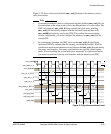
Table 2-2 and Table 2-3 list the smc_opmode0_<0-3> and SRAM Register settings. See
Register summary on page 3-3.
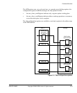
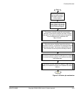
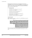
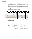
Figure 2-14 on page 2-29 shows a single asynchronous read transfer with an initial
access time, t
RC
, of three cycles and an output enable assertion delay, t
CEOE
, of one
cycle.
Table 2-2 Asynchronous read opmode chip register settings
Field mw rd_sync rd_bl wr_sync wr_bl baa adv bls ba
Value - b0 b000 - - - - - -
Table 2-3 Asynchronous read SRAM cycles register settings
Field t_rc t_wc t_ceoe t_wp t_pc t_tr
Value b0011 - b001 - - -