


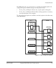

Functional Overview
ARM DDI 0389B Copyright © 2006 ARM Limited. All rights reserved. 2-27
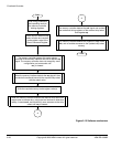
2.4.7 Interrupts operation
The next read to any chip select on the appropriate memory interface clears the
interrupt.
The interrupt outputs are generated through a combinational path from the relevant
input pin. This enables you to place the SMC in Low-power state, and to stop the clocks
while waiting for an interrupt.
When interrupts are disabled, a synchronized version of the interrupt input is still
readable through the APB interface.
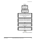
2.4.8 Memory interface operation
The memory interface issues commands to the memory from the command FIFO, and
controls the cycle timings of these commands. A new command is only issued when the
previous command is complete and any turn-around times have been met. Additionally,
a read command is not issued unless there is space for all the impending data in the read
data FIFO.
Note
You must not set the
rd_bl
parameter in the smc_opmode Register to a value greater
than the read data FIFO depth of four.
If enabled, the EBI can prevent commands being issued when the SMC is not granted
the external bus.
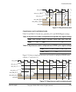
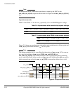
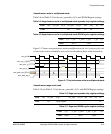
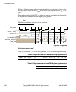
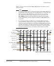
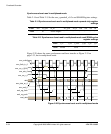
Figure 2-14 on page 2-29 to Figure 2-23 on page 2-38 show the timing parameters.
They are divided into SRAM timing tables and diagrams.
The internal signal read_data is included in the read transfer waveforms to indicate the
clock edge on which data is registered by the SMC.
SRAM timing tables and diagrams
All address, control, and write data outputs of the SMC are registered on the rising edge
of smc_mclk0n, equivalent to the falling edge of smc_mclk0, for both synchronous and
asynchronous accesses. The clock output to memory, smc_clk_out, is driven directly
by smc_mclk0, but gated to prevent toggling during asynchronous accesses, or when
no transfers are occurring.