


Programmer’s Model
3-2 Copyright © 2006 ARM Limited. All rights reserved. ARM DDI 0389B
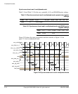
3.1 About the programmer’s model
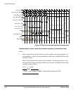
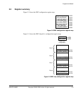
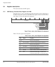
The SMC has 4KB of memory allocated to it from a base address of
0x1000
to a
maximum address of
0x1FFF
. Figure 3-1 shows that the register map address range is
split into the following regions:
SMC configuration registers
Use these registers for the global configuration, and control of operating
state, of the SMC.
SMC chip select configuration registers
These registers hold the operating parameters of each chip select.
SMC user configuration registers
These registers provide general purpose I/O for user specific
applications.
SMC integration test registers
Use these registers to verify correct integration of the SMC within a
system, by enabling non-AMBA ports to be set and read.
SMC PrimeCell Id registers
These registers enable the identification of system components by
software.
Figure 3-1 SMC register map
60&
3ULPH&HOO,'
60&
,QWHJUDWLRQWHVW
60&8VHUFIJ
60&&KLSFIJ
60&0HP&FIJ
[))&
[)(
[(
[
[
[