


Functional Overview
2-20 Copyright © 2006 ARM Limited. All rights reserved. ARM DDI 0389B
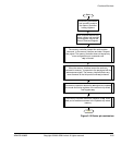
The SMC ensures the ordering of read transfers from a single port is maintained RAR,
and additionally that the ordering of write transfers from a single master is maintained
WAW.
SRAM memory accesses
This section describes:
• Standard SRAM access
• Memory address shifting
• Memory burst alignment
• Memory burst length on page 2-21
• Booting using the SRAM on page 2-21.
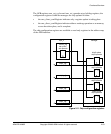
Standard SRAM access
The programmer’s view is a flat area of memory.
The base addresses of external memory devices are defined by the
smc_address_match0_<0-3>[7:0 ] and smc_address_mask0_<0-3>[ 7:0] tie-off
pins. You can read the values of these tie-off pins through the opmode registers.
Memory address shifting
To produce the address presented to the memory device, the AHB address is aligned to
the memory width. This is done because the AHB address is a byte-aligned address,
while the memory address is a memory-width-aligned address.
Note
During initial configuration of a memory device, the memory mode register can be
accessed with a sequence of transfers to specific addresses. You must take into
consideration the shifting performance by the SMC when accessing memory mode
registers.
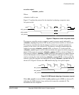
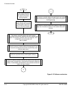
Memory burst alignment
The SMC provides a programmable option for controlling the formatting of memory
transfers with respect to memory burst boundaries, through the burst_align bit of the
opmode registers.
When set, the burst_align bit causes memory bursts to be aligned to a memory burst
boundary. This setting is intended for use with memories that use the concept of internal
pages. This can be an asynchronous page mode memory, or a synchronous PSRAM. If
a burst crosses a memory burst boundary, the SMC partitions the transfer into multiple