


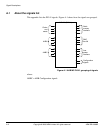

Signal Descriptions
ARM DDI 0389B Copyright © 2006 ARM Limited. All rights reserved. A-5
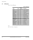
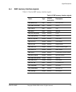
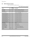
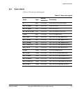
A.4 SMC memory interface signals
Table A-3 lists the SMC memory interface signals.
Table A-3 SMC memory interface signals
Name Type
Source/
destination
Description
smc_fbclk_in_0 Input Memory Fed back clock
smc_data_in_0[31:0] Input Memory Data in
smc_wait_0 Input Memory Wait
smc_int_0 Input Memory Interrupt
smc_clk_out_0[3:0] Output Memory Clock
smc_add_0[31:0] Output Memory Address
smc_cs_n_0[3:0] Output Memory Chip select
smc_we_n_0 Output Memory Write enable
smc_oe_n_0 Output Memory Output enable
smc_adv_n_0 Output Memory Address advance signal
smc_baa_n_0 Output Memory Bank address
smc_cre_0 Output Memory Configuration register enable
smc_bls_n_0[3:0] Output Memory Byte lane strobes
smc_data_out_0[31:0] Output Memory Data out
smc_data_en_0 Output Memory Data enable
smc_use_ebi Input Memory Use EBI tie-off
smc_ebigrant0 Input Memory EBI grant
smc_ebibackoff0 Input Memory EBI back off
smc_ebireq0 Output Memory EBI request