


Functional Overview
ARM DDI 0389B Copyright © 2006 ARM Limited. All rights reserved. 2-11
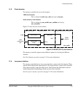
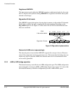
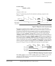
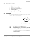
Figure 2-6 AHBC memory map
The other fourteen 4KB regions are read as zero. The lower 16 bits of the AHB address
decode the memory controller that is being used. An external AHB decoder determines
where in the system memory map, this 64KB region is located. See About the
programmer’s model on page 3-2 for information on the internal memory controller
configuration registers. The configuration port of the internal memory controller is
APB, so only word reads and writes are supported.
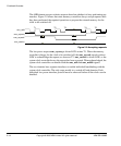
2.3.3 Clock domain operation
The memory controller supports two clock domains:
• the AHB clock domain
• the static memory clock domain.
The hclk input drives the AHB clock domain. This clock drives the AHB interfaces and
bus matrix. The static memory controller has a separate clock input in this domain. This
is called smc_aclk. This signal is separated to enable the clock to be stopped
independently of hclk for low-power operation, see Low-power interface operation on
page 2-12. These two clocks must always be driven from the same clock source. The
input signal hresetn resets this clock domain.
The static memory clock domain controls the memory interface logic of the SMC. The
input signal smc_mclk0 and its inverse smc_mclk0n drive this domain. Each external
static memory chip is driven by a gated smc_mclk0 signal, these are called
smc_clk_out_0[3:0]. Clocks are only driven out to chips that require them. The static
memory interface has a fed back clock input, smc_fbclk_in_0, to help with clock skews
on the external pads.
The memory controller supports many different options for clocking the different
domains:
5HVHUYHG
60&FRQILJ
[))))
5HDGDV]HUR
$+%&PHPRU\PDS
[
[
[