


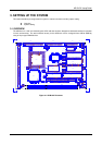

AR-B1474 User¡¦s Guide
2-7
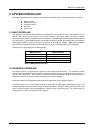
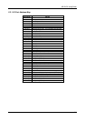
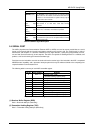
Name Description
-MASTER [Input] The MASTER is the signal from the I/O processor which
gains control as the master and should be held low for a
maximum of 15 microseconds or system memory may be
lost due to the lack of refresh
-MEMCS16
[Input, Open
collector]
The Memory Chip Select 16 indicates that the present
data transfer is a 1-wait state, 16-bit data memory
operation
-IOCS16
[Input, Open
collector]
The I/O Chip Select 16 indicates that the present data
transfer is a 1-wait state, 16-bit data I/O operation
OSC [Output] The Oscillator is a 14.31818 MHz signal
ZWS
[Input, Open
collector]
The Zero Wait State indicates to the microprocessor that
the present bus cycle can be completed without inserting
additional wait cycle
Table 2-6 ISA Bus Signal Description
2.4 SERIAL PORT
The ACEs (Asynchronous Communication Elements ACE1 to ACE2) are used to convert parallel data to a serial
format on the transmit side and convert serial data to parallel on the receiver side. The serial format, in order of
transmission and reception, is a start bit, followed by five to eight data bits, a parity bit (if programmed) and one,
one and half (five-bit format only) or two stop bits. The ACEs are capable of handling divisors of 1 to 65535, and
produce a 16x clock for driving the internal transmitter logic.
Provisions are also included to use this 16x clock to drive the receiver logic. Also included in the ACE a completed
MODEM control capability, and a processor interrupt system that may be software tailored to the computing time
required handle the communications link.
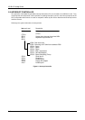
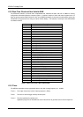
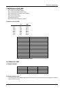
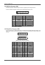
The following table is summary of each ACE accessible register
DLAB Port Address Register
Receiver buffer (read)0 base + 0
Transmitter holding register (write)
0 base + 1 Interrupt enable
X base + 2 Interrupt identification (read only)
X base + 3 Line control
X base + 4 MODEM control
X base + 5 Line status
X base + 6 MODEM status
X base + 7 Scratched register
1 base + 0 Divisor latch (least significant byte)
1 base + 1 Divisor latch (most significant byte)
Table 2-7 ACE Accessible Registers
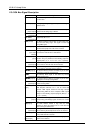
(1) Receiver Buffer Register (RBR)
Bit 0-7: Received data byte (Read Only)
(2) Transmitter Holding Register (THR)
Bit 0-7: Transmitter holding data byte (Write Only)