


AR-B1474 User¡¦s Guide
3-9
3.2.8 Memory Setting
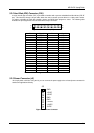
(1) Cache RAM Size Select (JP8)
The AR-B1474 can be configured to provide a write-back or write-through cache scheme and support 128KB to
512KB cache systems. A write-back cache system may provide better performance than a write-through cache
system. The BIOS Setup program allows you to set the cache scheme either write-back or write-through, either
the internal cache selection.
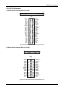
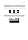
The AR-B1474 needs four 32Kx8 SRAM chips to construct 128KB cache. To construct 256KB cache, four 64Kx8
SRAM chips are needed. Four 128Kx8 SRAM chips will provide 512KB cache.
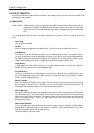
256KB
1 2
3 4
512KB
(Factory Preset)
128KB
1 2
3 4
1 2
3 4
JP8 JP8 JP8
Figure 3-15 JP8: Cache RAM Size Select
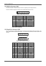
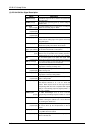
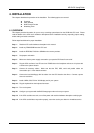
(3) DRAM Configuration
There is one 32-bit memory bank on the AR-B1474 card. It can be one-side or double-side SIMM (Single-Line
Memory Modules) which is designed to accommodate 256Kx36 bit to 8Mx36 bit SIMMs. This provides the user
with up to 32MB of main memory. The 32-bit SIMM (without parity bit) also can be used on AR-B1474 card. There
are six on-board memory configurations available. Please refer to the following table for details:
SIMM1 Total Memory
256KX32(X36) 1MB
512KX32(X36) 2MB
1MX32(X36) 4MB
2MX32(X36) 8MB
4MX32(X36) 16MB
8MX32(X36) 32MB
Table 3-7 DRAM Configuration