


SCPA033
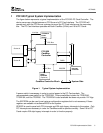
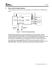
PCI1520 Implementation Guide 11
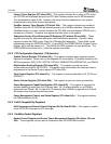
The EEPROM loading map can be found in the data manual. The following is an example data
file which could be loaded into the EEPROM for use with the PCI1520:
; EEPROM Programming Data for the PCI1520 Customer Board
; Configured for IRQ serialized interrupts and parallel PCI interrupts
; Register Data Description
00 0x01 ;Reference 1
01 0x03 ;04h Command Register, bit 8 (mapped from EEPROM bit 7), 6-5, 2-0
02 0x78 ;40h Sub-System Vendor ID Byte 0
03 0x56 ;40h Sub-System Vendor ID Byte 1
04 0x34 ;42h Sub-System ID Byte 0
05 0x12 ;42h Sub-System ID Byte 1
06 0xe0 ;44h Legacy Bar Byte 0, bits 7-1
07 0x03 ;44h Legacy Bar Byte 1
08 0x00 ;44h Legacy Bar Byte 2
09 0x00 ;44h Legacy Bar Byte 3
0a 0x60 ;80h System Control Byte 0 (default)
0b 0xd0 ;80h System Control Byte 1 (MRBURSTU=1 all others default)
0c 0x28 ;80h System Control Byte 3 (INTRTIE=1, P2CCLK=1)
0d 0x02 ;8ch MFUNC Byte 0 (MFUNC1=SDA, MFUNC0=INTA)
0e 0x10 ;8ch MFUNC Byte 1 (MFUNC3=IRQSER, MFUNC2=GPI2)
0f 0x00 ;8ch MFUNC Byte 2 (MFUNC5=GPI4, MFUNC4=SCL)
10 0x00 ;8ch MFUNC Byte 3 (MFUNC6=RSVD)
11 0xc0 ;90h Retry Status bits 7, 6 (PCI Retry, CardBus Retry)
12 0x00 ;91h Card Control bits 7, 5 (Ring Indicate Enable, ZV Port Select)
13 0x44 ;92h Dev Cntr bits 6, 3-0 (3V Capa, IRQ serialized and parallel PCI)
14 0x00 ;93h Diagnostic bits 7, 4-0
15 0x00 ;a2h Power Management Capabilities bit 15 (PME#_Supp from D3cold=0)
16 0x84 ;00h ExCA ID and Revision bits 7-0
17 0x00 ;Och+CB Socket Force Event Function 0 bit 27 (ZVSUPPORT=0)
18 0x00 ;Och+CB Socket Force Event Function 1 bit 27 (ZVSUPPORT=0)
8.2 BIOS Considerations
This section provides a high-level overview of the registers which need to be programmed by the
BIOS upon initialization. In general, the only registers which must be programmed for proper
operation within a Windows operating system are those registers which are EEPROM loadable.
Other registers may need to be changed according to system implementation. Microsoft
provides the following reference documents concerning initialization of CardBus controllers in
Windows:
http://www.microsoft.com/hwdev/bus/cardbus/cardbus1.asp
http://www.microsoft.com/hwdev/bus/pci/pcibridge-cardbus.asp
8.2.1 PCI Configuration Registers (Standard)
Cache Line Size Register (PCI offset 0Ch) – This register indicates the size in doublewords of
a cache line. This register is system architecture dependent.