


SCPA033
16 PCI1520 Implementation Guide
STOPCLK – Socket Control Register (CB offset 10h, bit 7). This bit determines whether the CB
CLKRUN# protocol is affected by the PCI CLKRUN# protocol.
CLKCTRLEN – Socket Power Management Register (CB offset 20h, bit 16). This bit enables
the CB CLKRUN# protocol.
CLKCTRL – Socket Power Management Register (CB offset 20h, bit 0). This bit determines
whether the CB CLKRUN# protocol will either stop or slow CCLK.
9.4 SUSPEND#
The assertion of the SUSPEND# signal gates PCLK, GRST#, PRST# from the PCI1520. The
recommended implementation for SUSPEND# is to not use it for power management and simply
connect a 43kΩ pullup resistor. SUSPEND# is an unstandardized method of power
management and causes many implementation problems. The following guidelines are
provided to help reduce implementation issues.
The main purpose of the PCI1520 SUSPEND# pin is to prevent PCI reset from clearing all
register context which would require the reconfiguration of the PCI1520 by software. Asserting
the PCI1520 SUSPEND# signal will also tri-state the controllers PCI outputs and gate the PCLK
internally to the controller if there isn't any PCI transaction currently in process. Due to the tri-
stated PCI outputs, it is important that the PCI bus not be parked on the PCI1520 when
SUSPEND# is asserted.
Another major point to note is that powerdown of a card slot due to card removal requires the
use of either the Internal Oscillator or an externally supplied clock to the power switch. If an
external clock is used and is removed during Suspend, the card slot will not power down and will
remain powered. This opens the possibility of potential card damage. If a 3.3V card is inserted
into the hot slot that was powered to 5V, card damage will most likely occur. It is therefore
recommended that P2CCLK, bit 27 at PCI offset 80h is set to a '1' so that the Internal Oscillator
is enabled. The CLOCK signal will then always be available as long as power is applied to the
CB controller.
10 Pin Compatibility with Other Devices
The PCI1520 is pin compatible with the PCI1620 PC Card, Flash Media, and Smart Card
Controller. This device has flash media and smart card terminals multiplexed on the PC Card
interface to allow for convenient access to many different media types. In order to design a PCB
for an upgrade path to the PCI1620, one change must be made from a normal PCI1520 PCB. A
48MHz clock is needed on the PCI1620. This clock input is located on pin 81 for the PDV
package and pin W11 for the GHK package.
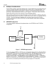
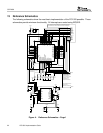
The PCI1520 can also be designed on to the same PCB as other Texas Instruments CardBus
controllers such as the single socket PCI1510 controller even though the two devices are not pin
compatible. This can be done using a dual footprint for the devices on the PCB. For example, a
designer may want the option of having a single or dual socket implementation on a single PCB.
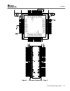
In this instance, a PCI1510 BGA (GGU) footprint can be placed inside a PCI1520 QFP (PDV)
footprint. The traces for the PC Card socket A on the PCI1520 footprint are then connected to
the PC Card socket traces on the PCI1510 footprint. For single socket implementations, only
one PC Card socket is populated along with the PCI1510 controller. For dual socket
implementation, both PC Card sockets are populated along with the PCI1520 controller.