


SCPA033
20 PCI1520 Implementation Guide
12 Migration to the PCI1420 from the PCI1225
The major differences between the PCI1420 and PCI1225 are the ability to wake from the D3
power state and the integration of the pullup resistors on the PC Card interface. This is done
using a global reset pin.
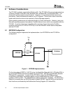
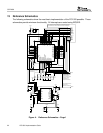
12.1 Hardware and Pin Assignment Changes
• The pinout changed slightly from the PCI1225 to the PCI1420. A VCC pin has been
replaced by a global reset pin (GRST#). This requires a PCB redesign. This pin allows
for wake from the D3 power state. Certain configuration registers are reset only by
GRST# and not PRST#. This allows the device to save context since PCI Reset must be
asserted on a D3 to D0 transition.
For systems requiring wake from D3, GRST# should be connected to a power-on reset
and PRST# should be connected to the system PCI Reset. When implementing GRST#
in this way, it must be treated similar to PRST# in that PCI Clock must be stable for
100µs before deassertion. The sequence of events should be: 1) Power on with GRST#
and PRST# asserted, 2) Clock becomes stable, 3) 100µs later GRST# can be
deasserted, 4) PRST# can be deasserted at the same time or any time after GRST# is
deasserted.
For systems not requiring wake from D3, GRST# can be tied to PRST# which is
connected to system PCI Reset. For more information, please refer to the datasheet and
the Section 9.1 – D3 Wake Information.
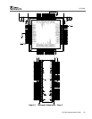
• All necessary pullup resistors on the PC Card interface have been integrated on the
PCI1420 with the exception of CCLKRUN#//WP(IOIS16#).