


SCPA033
4 PCI1520 Implementation Guide
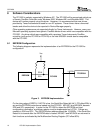
2 Power Considerations
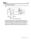
2.1 Internal Voltage Regulator
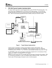
One of the major differences between the PCI1520 and previous Texas Instruments CardBus
controllers is that the PCI1520 uses an internal voltage regulator to power the core logic at 2.5V.
This allows for a more than 50% reduction in power consumption over previous controllers. The
voltage regulator is enabled using the VR_EN# pin. If VR_EN# is high, the voltage regulator is
disabled and VRPORT serves as a 2.5V external input to power the core. If VR_EN# is low, the
voltage regulator is enabled and VRPORT serves as a 2.5V output. This 2.5V output cannot be
used to power other devices and is only available externally in order to provide a 1µF bypass
capacitor. VRPORT must have a 1µF bypass capacitor to ground in order for proper operation if
the voltage regulator is enabled.
2.2 Clamping Rails
The PCI1520 has 3 clamping rails: VCCP, VCCA, and VCCB. VCCP is the PCI interface I/O
clamp rail and can be either 3.3V or 5V depending on the system implementation. The PCI1520
will only signal on the PCI bus at 3.3V but is 5V tolerant. VCCA and VCCB are connected to the
PC Card power rails for Socket A and Socket B, respectively. These terminals serve as the
clamping inputs for the PC Card interface to the PCI1520.
2.3 Bypass Capacitors
Standard design rules for power supply bypass should be followed. A value of 0.1µF is
recommended for each of the power pins VCC, VCCP, VCCA, and VCCB.