


SCPA033
PCI1520 Implementation Guide 5
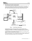
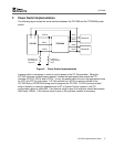
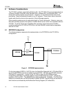
3 Power Switch Implementation
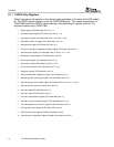
The following figure shows the serial interface between the PCI1520 and the TPS2226A power
switch:
VCCB
VPPB
Socket A
Pull-down for
I2C interface
(optional)
VPPA
CLOCK
PCI1520
LATCH
VCCA
TPS2226A
Socket B
VCCA
VCCB
DATA
Pulldown if
using internal
clock
Figure 2. Power Switch Implementation
A power switch is necessary in order to control power to the PC Card sockets. When the
PCI1520 receives a socket power request, it sends the appropriate data across the P
2
C
interface (CLOCK, DATA, and LATCH). In turn, the power switch turns on the appropriate levels
for VCC and VPP for that socket. A 2.7kΩ pulldown on LATCH is used to indicate to the
PCI1520 that an EEPROM is being used to program the PCI1520. CLOCK can be provided
either internally or externally depending on bit 27 in System Control register in the PCI
configuration space at offset 80h. If an external clock is used, the frequency should be between
32kHz and 100kHz. If the internal clock is used, a 43k pulldown resistor is necessary.