SP601 Hardware User Guide www.xilinx.com 11
UG518 (v1.1) August 19, 2009
Related Xilinx Documents
Block Diagram
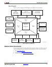
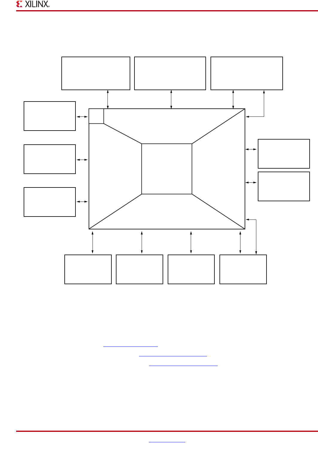
Figure 1-1 shows a high-level block diagram of the SP601 and its peripherals.
Related Xilinx Documents
Prior to using the SP601 Evaluation Board, users should be familiar with Xilinx resources.
See the following locations for additional documentation on Xilinx tools and solutions:
• ISE: www.xilinx.com/ise
• Answer Browser: www.xilinx.com/support
• Intellectual Property: www.xilinx.com/ipcenter
X-Ref Target - Figure 1-1
Figure 1-1: SP601 Features and Banking
LEDs
DIP Switch
GPIO Header
FMC LPC
Expansion Connector
10/100/1000
Ethernet GMII
Spartan-6
XC6SLX16
U1
Parallel Flash
USB
JTAG Connector
Pushbuttons
DDR2
Differential Clock
Clock Socket
SMA Clock
IIC EEPROM
and Header
MODE
DIP Switch
SPI x4 or
External Config
USB UART
UG518_01_070809
DED
Bank 0
2.5 V
Bank 3
1.8V
Bank 1
2.5V
Bank 2
2.5V


