42 www.xilinx.com SP601 Hardware User Guide
UG518 (v1.1) August 19, 2009
Chapter 1: SP601 Evaluation Board
Configuration Options
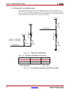
The FPGA on the SP601 Evaluation Board can be configured by the following methods:
• “3. SPI x4 Flash,” page 18
• “4. Linear Flash BPI,” page 20
• “JTAG Configuration,” page 42
For more information, refer to the Spartan-6 FPGA Configuration User Guide. [Ref 2]
JTAG Configuration
JTAG configuration is provided through onboard USB-to-JTAG configuration logic where
a computer host accesses the SP601 JTAG chain through a Type-A (computer host side) to
Type-Mini-B (SP601 side) USB cable.
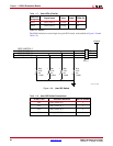
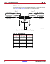
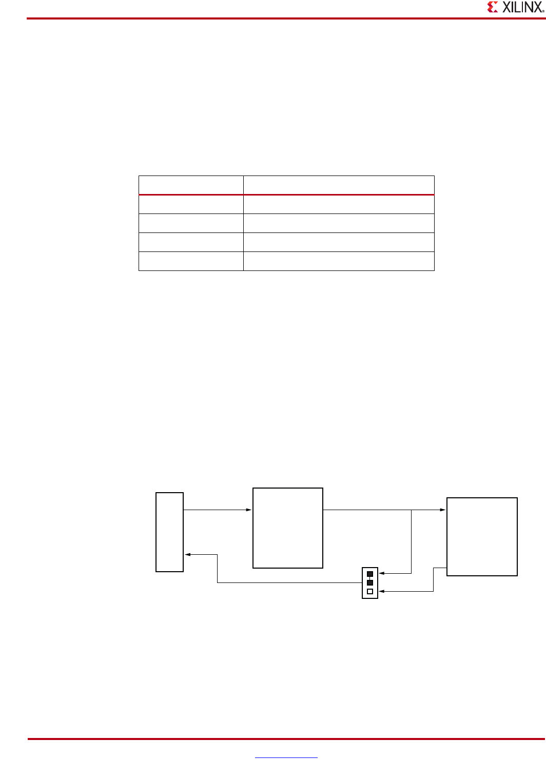
The JTAG chain of the board is illustrated in Figure 1-31. JTAG configuration is allowable
at any time under any mode pin setting. JTAG initiated configuration takes priority over
the mode pin settings.
FMC bypass jumper J4 must be connected between pins 1-2 for JTAG access to the FPGA
on the basic SP601 board, as shown in Figure 1-31. When the VITA 57.1 FMC expansion
connector is populated with an expansion module that has a JTAG chain, then jumper J4
must be set to connect pins 2-3 in order to include the FMC expansion module's JTAG
chain in the main SP601 JTAG chain.
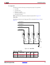
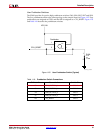
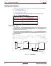
Table 1-23: Mode Pin Settings (M2 = 0)
Mode Pins (M1, M0) Configuration Mode
00 Master Byte Peripheral Interface (BPI)
01 Master SPI x1, x2, or x4
10 Not implemented on SP601
11 Not implemented on SP601
X-Ref Target - Figure 1-31
Figure 1-31: JTAG Chain
FMC LPC Expansion
TDI
TDI
TDO
TDO
J1
U1
J10
J4
FPGA
USB Mini-B
Connector
UG518_31_070809
*Default jumper setting excludes FMC.
To include FMC, jumper pins 2-3.
1


