21020285 D User’s Guide
Chapter 8 Details of Usage
Page 8 - 6 Byte and Word Swapping
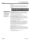
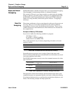
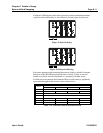
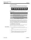
However, if you have an Intel processor, you must reinterpret the
representations in this manual to an order like this:
Note
Offset + x values are in
opposite order for Intel
Processors
In order for this transition to properly occur, more than just your interpretation
of the graphics in the manual must change. The RF3880 must be told to also
reinterpret the structures it uses.
RF3880
Swapping
Options
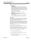
Byte and Word Swapping methodology for the RF3880 adapter is configured
with the Control field of the Address Buffer Port. This field is in the first word
written to the Address Buffer Port. (For bit-specific information on the Address
Buffer Port see Chapter 2, Hardware Essentials.)
Swapping is a function of the firmware on the RF3880 adapter and is enabled
and performed with minimal impact on performance.
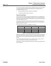
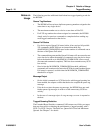
There are two bits in the Control field that allow you to separately control byte
swapping and word swapping. If you set neither of the swapping bits in the
Control field, the Command Structures will be ordered for a standard Motorola
processor.
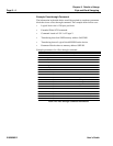
Command Structure Swapping
As explained, the need to byte-swap and word-swap the fields of the RF3880
Command Structures is due to the differences inherent in various processor
architectures. Since the RF3880 defaults to using Motorola ordering for its
structures, if your system uses a Motorola processor, no byte and word
swapping is necessary. However, if your system uses an Intel processor, the
Command Structures of the RF3880 must be adjusted.
This could be done entirely in software — the Host processor could re-order
the Command Structures. However this extra burden for the system is not
necessary because, by simply enabling the Byte and Word Swap controls, the
RF3880 adapter will automatically re-order the Command Structures.
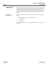
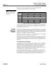
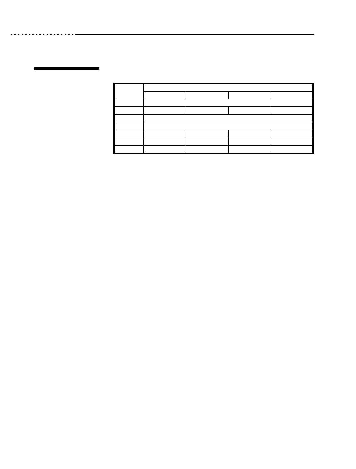
Address
Offset
Byte Memory Address
Offset + 3 Offset + 2 Offset + 1 Offset + 0
00H Command Identifier - 04030201H
04H Flags-2 = 01H Flags-1 = 86H Addr. Mod = 3EH Target ID = 02H
08H VME Memory Address - 005A9320H
0CH Transfer Count = 00010280H
10H 0 = 2AH 1 = 40H 2 = 0 3 = 08H
14H 4 = F4H 5 = E9H 6 = 0 7 = 02H
18H 8 = 05H 9 = 0 10 = 0 11 = 0
Table 112: Intel Ordered Parameter Block


