


Technical Reference Guide
Compaq Deskpro EXS and Workstation 300 Personal Computers
Featuring the Intel Pentium 4 Processor
First Edition - December 2000
3-3
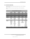
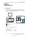
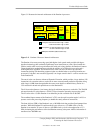
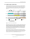
Figure 3-1 illustrates the internal architecture of the Pentium 4 processor.
Figure 3–2. Pentium 4 Processor Internal Architecture
The Pentium 4 increases processing speed with higher clock speeds made possible with hyper-
pipelined technology that can handle significantly more instructions at a time. Since branch mis-
predicts would result in serious performance hits with such a long pipeline, the Pentium 4 features
a branch prediction mechanism improved with the addition of an execution trace cache and a
refined prediction algorithm. The execution trace cache can store 12k micro-ops (decoded
instructions dealing with branching sequences) that are checked when re-occurring branches are
processed. Code that is not executed (bypassed) is no longer stored in the L1 cache as was the case
in the Pentium III.
The out-of-order core features Advanced Dynamic Execution, which provides a large window (126
instructions) for execution units to work with. A more accurate branch prediction algorithm, along
with a larger (4-KB) branch target buffer that stores more details on branch history results in a
33% reduction in branch mis-predictions over the Pentium III.
The L1 data cache features a low-latency design for minimum response to cache hits. The 256-KB
advanced transfer L2 cache features a 256-bit (32-byte) interface operating at processing speed.
The L2 cache of the 1.5 GHz Pentium 4 can therefore provide a transfer rate of 48 GB/s.
The combined improvements of the Pentium 4’s CPU core the rapid execution engine’s ALUs to
operate at twice the processing frequency to handle the steady stream of instructions.
The front side bus (FSB) of the Pentium 4 uses a 100-MHz clock but provides Quad-pumped data
transfers. While the Pentium III could transfer 8 bytes of data on a 133-MHz clock cycle the
Pentium 4 can transfer 32 bytes of data on a 100-MHz clock cycle for a throughput rate of 3.2
GB/s, balancing the performance of the dual-Rambus memory subsystem. Address information is
transferred at a 200-MHz rate.
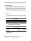
ALU Speed: 2.8 GHz w/Pentium 4 @ 1.4 GHz
3.0 GHz w/Pentium 4 @ 1.5 GHz
Core Speed: 1.4 GHz w/Pentium 4 @ 1.4 GHz
1.5 GHz w/Pentium 4 @ 1.5 GHz
FSB Speed: 400 MHz (Data transfer rate)
Pentium 4 Processor
128-bit
Integer
FPU
L1
Data
Cache
256-KB
8-Way
L2
Adv.
Transfer
Cache
FSB
I/F
Rapid Exe. Eng.
Branch
Prediction
CPU
ALUs
Execution
Trace Cache
Out-of-
Order Core