


Technical Reference Guide
Compaq Deskpro EXS and Workstation 300 Personal Computers
Featuring the Intel Pentium 4 Processor
First Edition - December 2000
4-7
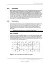
4.2.3 OPTION ROM MAPPING
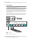
During POST, the PCI bus is scanned for devices that contain their own specific firmware in
ROM. Such option ROM data, if detected, is loaded into system memory’s DOS compatibility area
(refer to the system memory map shown in chapter 3).
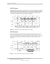
4.2.4 PCI INTERRUPTS
Eight interrupt signals (INTA- thru INTH-) are available for use by PCI devices. These signals
may be generated by on-board PCI devices or by devices installed in the PCI slots. For more
information on interrupts including PCI interrupt mapping refer to the “System Resources” section
4.4.
4.2.5 PCI POWER MANAGEMENT SUPPORT
This system complies with the PCI Power Management Interface Specification (rev 1.0). The PCI
Power Management Enable (PME-) signal is supported by the chipset and allows compliant PCI
and AGP peripherals to initiate the power management routine.
4.2.6 PCI SUB-BUSSES
The chipset implements two data busses that are supplementary in operation to the PCI bus:
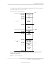
4.2.6.1 Hub Link Bus
The chipset implements a Hub Link bus between the MCH and the ICH. The Hub Link bus
handles transactions at a 66-MHz rate using PCI-type protocol, and in fact operates as PCI bus #0.
This bus is transparent to software and not accessible for expansion purposes.
4.2.6.2 LPC Bus
The 82801 ICH implements a Low Pin Count (LPC) bus for handling transactions to and from the
47B357 Super I/O Controller as well as the 82802 FWH. The LPC bus transfers data a nibble (4
bits) at a time at a 33-MHz rate. Generally transparent in operation, the LPC bus becomes a factor
primarily during the configuration of DMA channel modes (see section 4.4.3 “DMA”).