


M-LVDS Standard TIA/EIA−899
1-3
The M-LVDS Evaluation Module
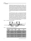
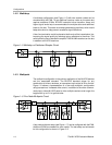
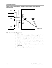
The EVM has been designed with the individual driver and receiver section
(SN75ALS180 footprint, U1) on one half of the board and the transceiver
section (SN75176 footprint, U2) on the other half (see Figure 3−1). The EVM
as delivered incorporates two 100-Ω termination resistors at each driver
output, receiver input, and transceiver I/O. These allow the user to evaluate
a single driver, receiver, or transceiver, while not having to deal with a
transmission line or additional I/Os.
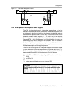
Jumpers are included to allow the two sections of the EVM to either share the
same power and ground or be run off of independent supplies. Ground shifts
or common-mode offsets can be introduced by the removal of these jumpers
and using separate power supplies.
1.2 M-LVDS Standard TIA/EIA−899
The M-LVDS standard was created in response to a demand from the data
communications community for a general-purpose high-speed balanced
interface standard for multipoint applications. The TIA/EIA−644 standard
defines the LVDS electrical-layer characteristics used for transmitting
information in point-to-point and multidrop architectures. TIA/EIA−644 does
not address data transmission for multipoint architectures, therefore the need
for development of a new standard.
The standard, Electrical Characteristics of Multipoint-Low-Voltage Differential
Signaling (M-LVDS) TIA/EIA−899, specifies low-voltage differential signaling
drivers and receivers for data interchange across half-duplex or multipoint
data bus structures. M-LVDS is capable of operating at signaling rates up to
500 Mbps. In other words, when the devices are used at the nominal signaling
rate, the rise and fall times will be within the specified values in the standard.
The M-LVDS standard defines the transition time (t
r
and t
f
) to be 1 ns or slower
into a test load. Using this information combined with the requirement that the
transition time not exceed 0.5 of the unit interval (UI), gives a minimum unit
interval of 2 ns, leading to the 500 Mpbs maximum signaling rate.
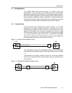
The standard defines Type-1 and Type-2 receivers. Type-1 receivers include
no provisions for failsafe and have their differential input voltage thresholds
near zero volts. Type-2 receivers have their differential input voltage
thresholds offset from zero volts to detect the absence of a voltage difference.
Type-1 receivers maximize the differential noise margin and are intended for
the maximum signaling rate. Type-2 receivers are intended for control signals,
slower signaling rates, or where failsafe provisions are needed. The bus
voltage logic state definition can be seen in Table 1−2 and Figure 1−2.