


PCB Construction
3-8
Bill of Materials, Board Layout, and PCB Construction
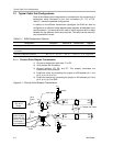
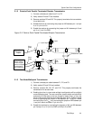
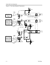
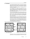
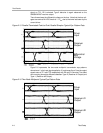
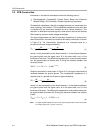
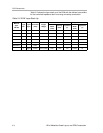
Table 3−2 shows the layer stack up of the EVM with the defined trace widths
for the controlled impedance etch runs using microstrip construction.
Table 3−2.EVM Layer Stack Up
Differential Model Single-Ended Model
Material
Type:
FR 406
Layer
No.
Layer
Type
Thickness
(mils)
Copper
Weight
Line
Width
(mils)
Spacing
(mils)
Impedance
(Ω)
Line
Width
(mils)
Impedance
(Ω)
1 Signal 0.0006 0.5 oz (start) 0.027 0.230 100 0.0420 50
PREPREG 0.025
2 Plane 0.0012 1
CORE 0.004
3 Plane 0.0012 1
PREPREG 0.025
4 Signal 0.0006 0.5 oz (start) 0.027 0.230 100 0.0420 50