


CY7C1246V18, CY7C1257V18
CY7C1248V18, CY7C1250V18
Document Number: 001-06348 Rev. *D Page 12 of 27
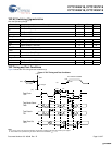
IEEE 1149.1 Serial Boundary Scan (JTAG)
These SRAMs incorporate a serial boundary scan test access
port (TAP) in the FBGA package. This part is fully compliant with
IEEE Standard #1149.1-2001. The TAP operates using JEDEC
standard 1.8V IO logic levels.
Disabling the JTAG Feature
It is possible to operate the SRAM without using the JTAG
feature. To disable the TAP controller, tie TCK LOW (V
SS
) to
prevent device clocking. TDI and TMS are internally pulled up
and may be unconnected. They may alternately be connected to
V
DD
through a pull up resistor. TDO must be left unconnected.
Upon power up, the device comes up in a reset state which does
not interfere with the operation of the device.
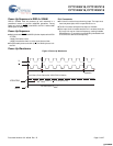
Test Access Port – Test Clock
The test clock is used only with the TAP controller. All inputs are
captured on the rising edge of TCK. All outputs are driven from
the falling edge of TCK.
Test Mode Select
The TMS input is used to give commands to the TAP controller
and is sampled on the rising edge of TCK. You can leave this pin
unconnected if the TAP is not used. The pin is pulled up inter-
nally, resulting in a logic HIGH level.
Test Data-In (TDI)
The TDI pin is used to serially input information into the registers
and can be connected to the input of any of the registers. The
register between TDI and TDO is chosen by the instruction that
is loaded into the TAP instruction register. For information about
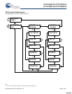
loading the instruction register, see “TAP Controller State
Diagram” on page 14. TDI is internally pulled up and can be
unconnected if the TAP is unused in an application. TDI is
connected to the most significant bit (MSB) on any register.
Test Data-Out (TDO)
The TDO output pin is used to serially clock data-out from the
registers. Whether the output is active depends on the current
state of the TAP state machine (see “Instruction Codes” on
page 17). The output changes on the falling edge of TCK. TDO
is connected to the least significant bit (LSB) of any register.
Performing a TAP Reset
A reset is performed by forcing TMS HIGH (V
DD
) for five rising
edges of TCK. This RESET does not affect the operation of the
SRAM and may be performed while the SRAM is operating. At
power up, the TAP is reset internally to ensure that TDO comes
up in a High-Z state.
TAP Registers
Registers are connected between the TDI and TDO pins and
scans data into and out of the SRAM test circuitry. Only one
register can be selected at a time through the instruction
registers. Data is serially loaded into the TDI pin on the rising
edge of TCK. Data is output on the TDO pin on the falling edge
of TCK.
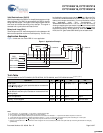
Instruction Register
Three-bit instructions can be serially loaded into the instruction
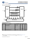
register. This register is loaded when it is placed between the TDI
and TDO pins as shown in “TAP Controller Block Diagram” on
page 15. Upon power up, the instruction register is loaded with
the IDCODE instruction. It is also loaded with the IDCODE
instruction if the controller is placed in a reset state as described
in the previous section.
When the TAP controller is in the Capture-IR state, the two least
significant bits are loaded with a binary ‘01’ pattern to enable fault
isolation of the board level serial test path.
Bypass Register
To save time when serially shifting data through registers, it is
sometimes advantageous to skip certain chips. The bypass
register is a single-bit register that can be placed between TDI
and TDO pins. This shifts data through the SRAM with minimal
delay. The bypass register is set LOW (V
SS
) when the BYPASS
instruction is executed.
Boundary Scan Register
The boundary scan register is connected to all of the input and
output pins on the SRAM. Several no connect (NC) pins are also
included in the scan register to reserve pins for higher density
devices.
The boundary scan register is loaded with the contents of the
RAM input and output ring when the TAP controller is in the
Capture-DR state and is then placed between the TDI and TDO
pins when the controller is moved to the Shift-DR state. The
EXTEST, SAMPLE/PRELOAD, and SAMPLE Z instructions can
be used to capture the contents of the input and output ring.
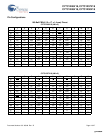
“Boundary Scan Order” on page 18 shows the order in which the
bits are connected. Each bit corresponds to one of the bumps on
the SRAM package. The MSB of the register is connected to TDI,
and the LSB is connected to TDO.
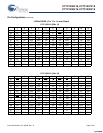
Identification (ID) Register
The ID register is loaded with a vendor-specific, 32-bit code
during the Capture-DR state when the IDCODE command is
loaded in the instruction register. The IDCODE is hardwired into
the SRAM and can be shifted out when the TAP controller is in
the Shift-DR state. The ID register has a vendor code and other
information described in “Identification Register Definitions” on
page 17.
TAP Instruction Set
Eight different instructions are possible with the three-bit
instruction register. All combinations are listed in “Instruction
Codes” on page 17. Three of these instructions are listed as
RESERVED and must not be used. The other five instructions
are described in this section in detail.
Instructions are loaded into the TAP controller during the Shift-IR
state when the instruction register is placed between TDI and
TDO. During this state, instructions are shifted through the
instruction register through the TDI and TDO pins. To execute
the instruction after it is shifted in, the TAP controller must be
moved into the Update-IR state.
[+] Feedback [+] Feedback