


CY7C1246V18, CY7C1257V18
CY7C1248V18, CY7C1250V18
Document Number: 001-06348 Rev. *D Page 9 of 27
Valid Data Indicator (QVLD)
QVLD is provided on the DDR-II+ to simplify data capture on high
speed systems. The QVLD is generated by the DDR-II+ device
along with data output. This signal is also edge aligned with the
echo clock and follows the timing of any data pin. This signal is
asserted half a cycle before valid data arrives.
Delay Lock Loop (DLL)
These chips use a DLL that is designed to function between 120
MHz and the specified maximum clock frequency. The DLL may
be disabled by applying ground to the DOFF pin. When the DLL
is turned off, the device behaves in DDR-I mode (with 1.0 cycle
latency and a longer access time). For more information, refer to
the application note, DLL Considerations in
QDRII/DDRII/QDRII+/DDRII+. The DLL can also be reset by
slowing or stopping the input clocks K and K
for a minimum of 30
ns. However, it is not necessary for the DLL to be reset to lock to
the desired frequency. During power up, when the DOFF
is tied
HIGH, the DLL gets locked after 2048 cycles of stable clock.
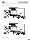
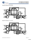
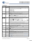
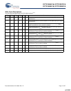
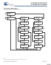
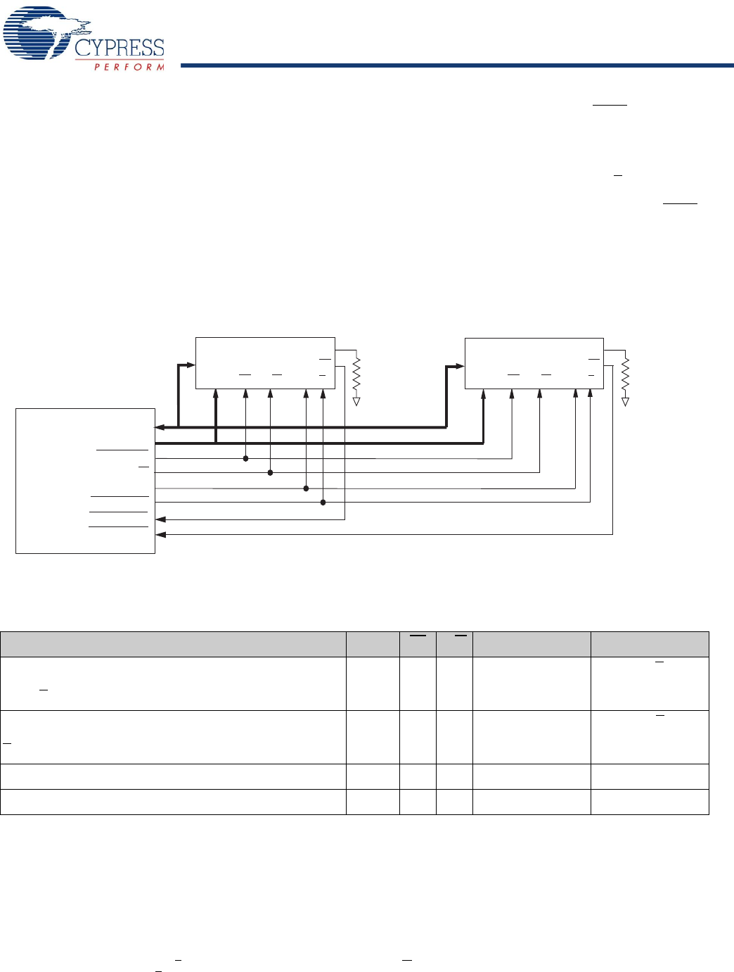
Application Example
Figure 1 shows the use of two DDR-II+ in an application.
Figure 1. Application Example
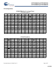
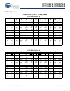
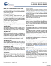
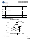
Truth Table
The truth table for the CY7C1246V18, CY7C1257V18, CY7C1248V18, and CY7C1250V18 follows.
[2, 3, 4, 5, 6, 7]
Operation K LD R/W DQ DQ
Write Cycle:
Load address; wait one cycle; input write data on consecutive
K and K
rising edges.
L-H L L D(A) at K(t + 1) ↑ D(A + 1) at K(t + 1) ↑
Read Cycle: (2.0 cycle Latency)
Load address; wait two cycle; read data on consecutive K and
K rising edges.
L-H L H Q(A) at K(t + 2) ↑ Q(A + 1) at K
(t + 2) ↑
NOP: No Operation L-H H X High-Z High-Z
Standby: Clock Stopped Stopped X X Previous State Previous State
BUS
MASTER
(CPU or ASIC)
DQ
Addresses
Cycle Start
R/W
Source CLK
Source CLK
Echo Clock1/Echo Clock1
Echo Clock2/Echo Clock2
R = 250ohms
LD R/W
DQ
A
SRAM#1
K
ZQ
CQ/CQ
K
R = 250ohms
LD R/W
DQ
A
SRAM#2
K
ZQ
CQ/CQ
K
Notes
2. X = “Don’t Care,” H = Logic HIGH, L = Logic LOW, ↑
represents rising edge.
3. Device powers up deselected with the outputs in a tri-state condition.
4. “A” represents address location latched by the devices when transaction was initiated. A + 1 represents the address sequence in the burst.
5. “t” represents the cycle at which a read/write operation is started. t + 1 and t + 2 are the first and second clock cycles succeeding the “t” clock cycle.
6. Data inputs are registered at K and K
rising edges. Data outputs are delivered on K and K rising edges.
7. Cypress recommends that K = K
= HIGH when clock is stopped. This is not essential, but permits most rapid restart by overcoming transmission line charging
symmetrically.
[+] Feedback [+] Feedback