


CY7C1246V18, CY7C1257V18
CY7C1248V18, CY7C1250V18
Document Number: 001-06348 Rev. *D Page 21 of 27
\
Capacitance
Tested initially and after any design or process change that may affect these parameters.
Parameter Description Test Conditions Max Unit
C
IN
Input Capacitance T
A
= 25°C, f = 1 MHz,
V
DD
= 1.8V
V
DDQ
= 1.5V
5pF
C
CLK
Clock Input Capacitance 4 pF
C
O
Output Capacitance 5 pF
Thermal Resistance
Tested initially and after any design or process change that may affect these parameters.
Parameter Description Test Conditions
165 FBGA
Package
Unit
Θ
JA
Thermal Resistance
(Junction to Ambient)
Test conditions follow standard test methods and
procedures for measuring thermal impedance, per
EIA/JESD51.
16.25 °C/W
Θ
JC
Thermal Resistance
(Junction to Case)
2.91 °C/W
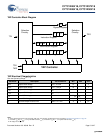
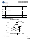
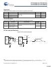
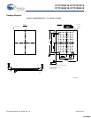
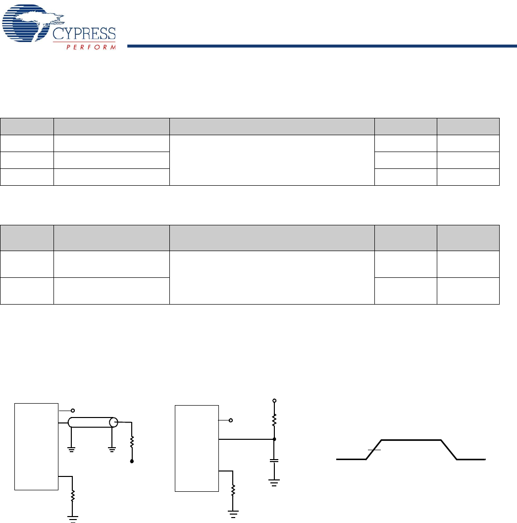
AC Test Loads and Waveforms
Figure 4. AC Test Loads and Waveforms
1.25V
0.25V
R = 50Ω
5pF
INCLUDING
JIG AND
SCOPE
ALL INPUT PULSES
Device
R
L
= 50Ω
Z
0
= 50Ω
V
REF
= 0.75V
V
REF
= 0.75V
[20]
0.75V
Under
Test
0.75V
Device
Under
Test
OUTPUT
0.75V
V
REF
V
REF
OUTPUT
ZQ
ZQ
(a)
Slew Rate = 2 V/ns
RQ =
250
Ω
(b)
RQ =
250
Ω
Note
20.Unless otherwise noted, test conditions assume signal transition time of 2V/ns, timing reference levels of 0.75V, V
REF
= 0.75V, RQ = 250Ω, V
DDQ
= 1.5V, input
pulse levels of 0.25V to 1.25V, and output loading of the specified I
OL
/I
OH
and load capacitance shown in (a) of AC Test Loads and Waveforms.
[+] Feedback [+] Feedback