


CY7C1246V18, CY7C1257V18
CY7C1248V18, CY7C1250V18
Document Number: 001-06348 Rev. *D Page 20 of 27
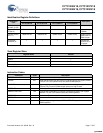
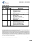
Maximum Ratings
Exceeding maximum ratings may impair the useful life of the
device. These user guidelines are not tested.
Storage Temperature ................................ –65°C to + 150°C
Ambient Temperature with Power Applied. –55°C to + 125°C
Supply Voltage on V
DD
Relative to GND.......–0.5V to + 2.9V
Supply Voltage on V
DDQ
Relative to GND..... –0.5V to + V
DD
DC Applied to Outputs in High-Z .........–0.5V to V
DDQ
+ 0.3V
DC Input Voltage
[11]
...............................–0.5V to V
DD
+ 0.3V
Current into Outputs (LOW).........................................20 mA
Static Discharge Voltage (MIL-STD-883, M 3015).... >2001V
Latch up Current..................................................... >200 mA
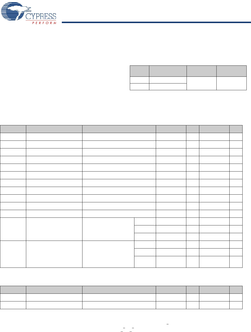
Operating Range
Range
Ambient
Temperature V
DD
[15]
V
DDQ
[15]
Com’l 0°C to +70°C 1.8 ± 0.1V 1.4V to V
DD
Ind’l –40°C to +85°C
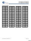
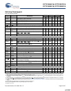
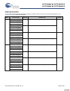
Electrical Characteristics
Over the Operating Range
[12]
DC Electrical Characteristics
Parameter Description Test Conditions Min Typ Max Unit
V
DD
Power Supply Voltage 1.7 1.8 1.9 V
V
DDQ
IO Supply Voltage 1.4 1.5 V
DD
V
V
OH
Output HIGH Voltage Note 16 V
DDQ
/2 – 0.12 V
DDQ
/2 + 0.12 V
V
OL
Output LOW Voltage Note 17 V
DDQ
/2 – 0.12 V
DDQ
/2 + 0.12 V
V
OH(LOW)
Output HIGH Voltage I
OH
= –0.1 mA, Nominal Impedance V
DDQ
– 0.2 V
DDQ
V
V
OL(LOW)
Output LOW Voltage I
OL
= 0.1 mA, Nominal Impedance V
SS
0.2 V
V
IH
Input HIGH Voltage V
REF
+ 0.1 V
DDQ
+ 0.15 V
V
IL
Input LOW Voltage –0.15 V
REF
– 0.1 V
I
X
Input Leakage Current GND ≤ V
I
≤ V
DDQ
–2 2 μA
I
OZ
Output Leakage Current GND ≤ V
I
≤ V
DDQ,
Output Disabled –2 2 μA
V
REF
Input Reference Voltage
[18]
Typical Value = 0.75V 0.68 0.75 0.95 V
I
DD
[19]
V
DD
Operating Supply V
DD
= Max., I
OUT
= 0 mA,
f = f
MAX
= 1/t
CYC
300 MHz 1000 mA
333 MHz 1080 mA
375 MHz 1210 mA
I
SB1
Automatic Power Down
Current
Max. V
DD
,
Both Ports Deselected,
V
IN
≥ V
IH
or V
IN
≤ V
IL
f = f
MAX
= 1/t
CYC
,
Inputs Static
300 MHz 290 mA
333 MHz 300 mA
375 MHz 320 mA
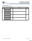
AC Input Requirements
Over the Operating Range
[11]
Parameter Description Test Conditions Min Typ. Max Unit
V
IH
Input HIGH Voltage V
REF
+ 0.2 – V
DDQ
+ 0.24 V
V
IL
Input LOW Voltage –0.24 – V
REF
– 0.2 V
Notes
15.Power up: assumes a linear ramp from 0V to V
DD
(min) within 200 ms. During this time V
IH
< V
DD
and V
DDQ
< V
DD
.
16.Outputs are impedance controlled. I
OH
= –(V
DDQ
/2)/(RQ/5) for values of 175Ω < RQ < 350Ω.
17.Outputs are impedance controlled. I
OL
= (V
DDQ
/2)/(RQ/5) for values of 175Ω < RQ < 350Ω.
18.V
REF
(min) = 0.68V or 0.46V
DDQ
, whichever is larger. V
REF
(max) = 0.95V or 0.54V
DDQ
, whichever is smaller.
19.The operation current is calculated with 50% read cycle and 50% write cycle.
[+] Feedback [+] Feedback