


CY7C1246V18, CY7C1257V18
CY7C1248V18, CY7C1250V18
Document Number: 001-06348 Rev. *D Page 23 of 27
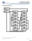
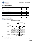
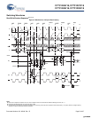
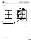
Switching Waveforms
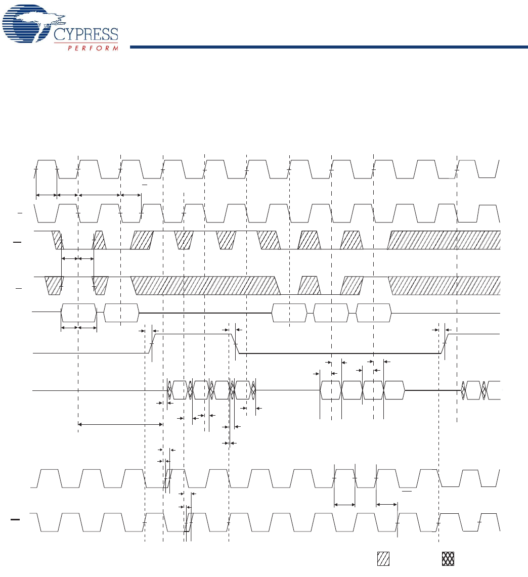
Read/Write/Deselect Sequence
[28, 29, 30]
Figure 5. Waveform for 2.0 Cycle Read Latency
DON’T CARE UNDEFINED
1
2
3
4
5
6
7
8
9
10
READ
READ
READ NOP WRITE
WRITE
t
NOP
11
K
K
LD
R/W
A
t
KH
t
KL
t
CYC
t
HC
t
SA
t
HA
SC
A0
A1
A2
A3
A4
CQ
CQ
QVLD
QVLD
t
NOP
t
QVLD
t
t
CCQO
t
CQOH
t
t
CQOH
QVLD
t
NOP
DQ
KHKH
12
(Read Latency = 2.0 Cycles)
NOP
NOP
CCQO
t
SD
HD
t
SD
t
HD
t
CLZ
t
CHZ
D20
D21
D30
D31
t
CQDOH
Q00
Q11
Q01
Q10
t
DOH
t
CO
Q40
Q41
t
CQD
t
t
t
CQH
CQHCQH
Notes
28.Q00 refers to output from address A0. Q01 refers to output from the next internal burst address following A0, that is, A0 + 1.
29.Outputs are disabled (High-Z) one clock cycle after a NOP.
30.The third NOP cycle between read to write transition is not necessary for correct device operation when Read Latency = 2.0 cycles; however at high frequency
operation, it may be required to avoid bus contention.
[+] Feedback [+] Feedback