


CY7C1246V18, CY7C1257V18
CY7C1248V18, CY7C1250V18
Document Number: 001-06348 Rev. *D Page 8 of 27
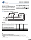
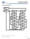
Functional Overview
The CY7C1246V18, CY7C1257V18, CY7C1248V18, and
CY7C1250V18 are synchronous pipelined Burst SRAMs
equipped with a DDR interface.
Accesses for both ports are initiated on the Positive Input Clock
(K). All synchronous input and output timing refer to the rising
edge of the input clocks (K and K).
All synchronous data inputs (D
[x:0]
) pass through input registers
controlled by the rising edge of the input clocks (K and K
). All
synchronous data outputs (Q
[x:0]
) pass through output registers
controlled by the rising edge of the input clocks (K and K
).
All synchronous control (R/W, LD, BWS
[0:X]
) inputs pass through
input registers controlled by the rising edge of the input clock
(K\K).
CY7C1248V18 is described in the following sections. The same
basic descriptions apply to CY7C1246V18, CY7C1257V18, and
CY7C1250V18.
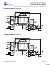
Read Operations
The CY7C1248V18 is organized internally as a single array of
2M x 18. Accesses are completed in a burst of two sequential
18-bit data words. Read operations are initiated by asserting
R/W
HIGH and LD LOW at the rising edge of the positive input
clock (K). Following the next two K clock rising edges, the corre-
sponding 18-bit word of data from this address location is driven
onto the Q
[17:0]
using K as the output timing reference. On the
subsequent rising edge of K
the next 18-bit data word is driven
onto the Q
[17:0]
. The requested data is valid 0.45 ns from the
rising edge of the input clock (K and K
). To maintain the internal
logic, each read access must be allowed to complete. Read
accesses can be initiated on every rising edge of the positive
input clock (K).
When read access is deselected, the CY7C1248V18 completes
the pending read transactions. Synchronous internal circuitry
automatically tri-states the outputs following the next rising edge
of the positive input clock (K). This enables a seamless transition
between devices without the insertion of wait states in a depth
expanded memory.
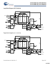
Write Operations
Write operations are initiated by asserting R/W
LOW and LD
LOW at the rising edge of the positive input clock (K). The
address presented to Address inputs is stored in the Write
Address register. On the following K clock rise, the data
presented to D
[17:0]
is latched and stored into the 18-bit Write
Data register, provided BWS
[1:0]
are both asserted active. On the
subsequent rising edge of the Negative Input Clock (K
), the infor-
mation presented to D
[17:0]
is also stored into the Write Data
register, provided BWS
[1:0]
are both asserted active. The 36 bits
of data are then written into the memory array at the specified
location. Write accesses can be initiated on every rising edge of
the positive input clock (K). Doing so pipelines the data flow such
that 18 bits of data can be transferred into the device on every
rising edge of the input clocks (K and K
).
When write access is deselected, the device ignores all inputs
after the pending write operations are completed.
Byte Write Operations
Byte write operations are supported by the CY7C1248V18. A
write operation is initiated as described in the Write Operations
section. The bytes that are written are determined by BWS
0
and
BWS
1
, which are sampled with each set of 18-bit data words.
Asserting the appropriate Byte Write Select input during the data
portion of a write latches the data being presented and written
into the device. Deasserting the Byte Write Select input during
the data portion of a write enables the data stored in the device
for that byte to remain unaltered. This feature can be used to
simplify read/modify/write operations to a byte write operation.
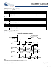
Double Data Rate Operation
The CY7C1248V18 enables high-performance operation
through high clock frequencies (achieved through pipelining) and
DDR mode of operation. The CY7C1248V18 requires two No
Operation (NOP) cycles when transitioning from a read to a write
cycle. At higher frequencies, some applications may require a
third NOP cycle to avoid contention.
If a read occurs after a write cycle, address and data for the write
are stored in registers. The write information must be stored
because the SRAM cannot perform the last word write to the
array without conflicting with the read. The data stays in this
register until the next write cycle occurs. On the first write cycle
after the read(s), the stored data from the earlier write is written
into the SRAM array. This is called a Posted Write.
If a read is performed on the same address on which a write is
performed in the previous cycle, the SRAM reads out the most
current data. The SRAM does this by bypassing the memory
array and reading the data from the registers.
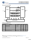
Depth Expansion
Depth expansion requires replicating the LD control signal for
each bank. All other control signals can be common between
banks as appropriate.
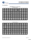
Programmable Impedance
An external resistor, RQ, must be connected between the ZQ pin
on the SRAM and V
SS
to enable the SRAM to adjust its output
driver impedance. The value of RQ must be 5x the value of the
intended line impedance driven by the SRAM. The allowable
range of RQ to guarantee impedance matching with a tolerance
of ±15%, is between 175Ω and 350Ω
, with V
DDQ
=1.5V. The
output impedance is adjusted every 1024 cycles upon power up
to account for drifts in supply voltage and temperature.
Echo Clocks
Echo clocks are provided on the DDR-II+ to simplify data capture
on high speed systems. Two echo clocks are generated by the
DDR-II+. CQ is referenced with respect to K and CQ
is refer-
enced with respect to K
. These are free-running clocks and are
synchronized to the input clock of the DDR-II+. The timing for the
echo clocks is shown in “Switching Characteristics” on page 22.
[+] Feedback [+] Feedback