


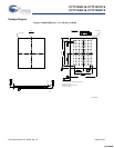
Document Number: 001-06348 Rev. *D Revised March 11, 2008 Page 27 of 27
All product and company names mentioned in this document are the trademarks of their respective holders.
CY7C1246V18, CY7C1257V18
CY7C1248V18, CY7C1250V18
© Cypress Semiconductor Corporation, 2006-2008. The information contained herein is subject to change without notice. Cypress Semiconductor Corporation assumes no responsibility for the use of
any circuitry other than circuitry embodied in a Cypress product. Nor does it convey or imply any license under patent or other rights. Cypress products are not warranted nor intended to be used for
medical, life support, life saving, critical control or safety applications, unless pursuant to an express written agreement with Cypress. Furthermore, Cypress does not authorize its products for use as
critical components in life-support systems where a malfunction or failure may reasonably be expected to result in significant injury to the user. The inclusion of Cypress products in life-support systems
application implies that the manufacturer assumes all risk of such use and in doing so indemnifies Cypress against all charges.
Any Source Code (software and/or firmware) is owned by Cypress Semiconductor Corporation (Cypress) and is protected by and subject to worldwide patent protection (United States and foreign),
United States copyright laws and international treaty provisions. Cypress hereby grants to licensee a personal, non-exclusive, non-transferable license to copy, use, modify, create derivative works of,
and compile the Cypress Source Code and derivative works for the sole purpose of creating custom software and or firmware in support of licensee product to be used only in conjunction with a Cypress
integrated circuit as specified in the applicable agreement. Any reproduction, modification, translation, compilation, or representation of this Source Code except as specified above is prohibited without
the express written permission of Cypress.
Disclaimer: CYPRESS MAKES NO WARRANTY OF ANY KIND, EXPRESS OR IMPLIED, WITH REGARD TO THIS MATERIAL, INCLUDING, BUT NOT LIMITED TO, THE IMPLIED WARRANTIES
OF MERCHANTABILITY AND FITNESS FOR A PARTICULAR PURPOSE. Cypress reserves the right to make changes without further notice to the materials described herein. Cypress does not
assume any liability arising out of the application or use of any product or circuit described herein. Cypress does not authorize its products for use as critical components in life-support systems where
a malfunction or failure may reasonably be expected to result in significant injury to the user. The inclusion of Cypress’ product in a life-support systems application implies that the manufacturer
assumes all risk of such use and in doing so indemnifies Cypress against all charges.
Use may be limited by and subject to the applicable Cypress software license agreement.
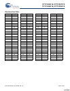
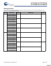
Document History Page
Document Title: CY7C1246V18/CY7C1257V18/CY7C1248V18/CY7C1250V18, 36-Mbit DDR-II+ SRAM 2-Word Burst Ar-
chitecture (2.0 Cycle Read Latency)
Document Number: 001-06348
REV. ECN No. Issue Date
Orig. of
Change
Description of Change
** 425689 See ECN NXR New Data Sheet
*A 461639 See ECN NXR Revised the MPNs from
CY7C1257AV18 to CY7C1257V18
CY7C1248AV18 to CY7C1248V18
CY7C1250AV18 to CY7C1250V18
Changed t
TH
and t
TL
from 40 ns to 20 ns, changed t
TMSS
, t
TDIS
, t
CS
, t
TMSH
,
t
TDIH
, t
CH
from
10 ns to 5 ns and changed t
TDOV
from 20 ns to 10 ns in TAP
AC Switching Characteristics table
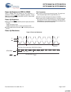
Modified Power-Up waveform
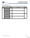
*B 497628 See ECN NXR Changed the V
DDQ
operating voltage to 1.4V to V
DD
in the Features section,
in Operating Range table and in the DC Electrical Characteristics table
Added foot note in page# 1
Changed the Maximum rating of Ambient Temperature with Power Applied
from –10°C to +85°C to –55°C to +125°C
Changed V
REF
(Max.) spec from 0.85V to 0.95V in the DC Electrical
Characteristics table and in the note below the table
Updated foot note #17 to specify Overshoot and Undershoot Spec
Updated Θ
JA
and Θ
JC
values
Removed x9 part and its related information
Updated footnote #24
*C 1093183 See ECN VKN Converted from preliminary to final
Added x8 and x9 parts
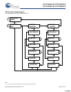
Updated logic block diagram for x18 and x36 parts
Changed I
DD
values from 925 mA to 1210 mA for 375 MHz, 800 mA to 1080
mA for 333 MHz, 725 mA to 1000 mA for 300 MHz
Changed I
SB
values from 290 mA to 320 mA for 375 MHz, 270 mA to 300
mA for 333 MHz, 250 mA to 290 mA for 300 MHz
Changed Θ
JA
value from 12.43 °C/W to 16.25 °C/W
Changed t
CYC
max spec to 8.4 ns for all speed bins
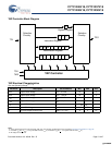
Updated Ordering Information table
*D 2198506 See ECN VKN/AESA Added footnote# 19 related to I
DD
[+] Feedback [+] Feedback