


CY7C1246V18, CY7C1257V18
CY7C1248V18, CY7C1250V18
Document Number: 001-06348 Rev. *D Page 17 of 27
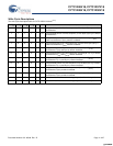
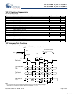
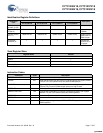
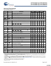
Identification Register Definitions
Instruction
Field
Value
Description
CY7C1246V18 CY7C1257V18 CY7C1248V18 CY7C1250V18
Revision
Number (31:29)
000 000 000 000 Version number.
Cypress Device
ID (28:12)
11010111100000111 11010111100001111 11010111100010111 11010111100100111 Defines the type
of SRAM.
Cypress JEDEC
ID (11:1)
00000110100 00000110100 00000110100 00000110100 Enables unique
identification of
SRAM vendor.
ID Register
Presence (0)
1 1 1 1 Indicates the
presence of an
ID register.
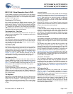
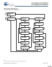
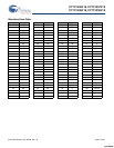
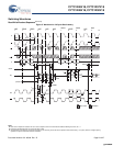
Scan Register Sizes
Register Name Bit Size
Instruction 3
Bypass 1
ID 32
Boundary Scan 109
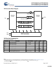
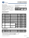
Instruction Codes
Instruction Code Description
EXTEST 000 Captures the input/output ring contents.
IDCODE 001 Loads the ID register with the vendor ID code and places the register between
TDI and TDO. This operation does not affect SRAM operation.
SAMPLE Z 010 Captures the input/output contents. Places the boundary scan register between
TDI and TDO. Forces all SRAM output drivers to a High-Z state.
RESERVED 011 Do Not Use: This instruction is reserved for future use.
SAMPLE/PRELOAD 100 Captures the input/output ring contents. Places the boundary scan register
between TDI and TDO. Does not affect the SRAM operation.
RESERVED 101 Do Not Use: This instruction is reserved for future use.
RESERVED 110 Do Not Use: This instruction is reserved for future use.
BYPASS 111 Places the bypass register between TDI and TDO. This operation does not affect
SRAM operation.
[+] Feedback [+] Feedback