


CY7C1246V18, CY7C1257V18
CY7C1248V18, CY7C1250V18
Document Number: 001-06348 Rev. *D Page 7 of 27
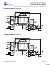
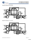
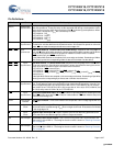
ZQ Input Output Impedance Matching Input. This input is used to tune the device outputs to the system
data bus impedance. CQ, CQ
, and Q
[x:0]
output impedance are set to 0.2 x RQ, where RQ is a
resistor connected between ZQ and ground. Alternatively, this pin can be connected directly to
V
DDQ
, which enables the minimum impedance mode. This pin cannot be connected directly to
GND or left unconnected.
DOFF
Input DLL Turn Off, Active LOW. Connecting this pin to ground turns off the DLL inside the device.
The timing in the DLL turned off operation is different from that listed in this data sheet. For
normal operation, this pin can be connected to a pull up through a 10 Kohm or less pull up
resistor. The device behaves in DDR-I mode when the DLL is turned off. In this mode, the device
can be operated at a frequency of up to 167 MHz with DDR-I timing.
TDO Output TDO for JTAG.
TCK Input TCK Pin for JTAG.
TDI Input TDI Pin for JTAG.
TMS Input TMS Pin for JTAG.
NC N/A Not Connected to the Die. Can be tied to any voltage level.
NC/72M N/A Not Connected to the Die. Can be tied to any voltage level.
NC/144M N/A Not Connected to the Die. Can be tied to any voltage level.
NC/288M N/A Not Connected to the Die. Can be tied to any voltage level.
V
REF
Input-
Reference
Reference Voltage Input. Static input used to set the reference level for HSTL inputs, outputs,
and AC measurement points.
V
DD
Power Supply Power Supply Inputs to the Core of the Device.
V
SS
Ground Ground for the Device.
V
DDQ
Power Supply Power Supply Inputs for the Outputs of the Device.
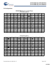
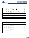
Pin Definitions (continued)
Pin Name IO Pin Description
[+] Feedback [+] Feedback