


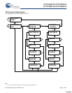

CY7C1246V18, CY7C1257V18
CY7C1248V18, CY7C1250V18
Document Number: 001-06348 Rev. *D Page 6 of 27
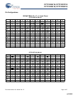
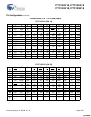
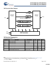
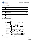
Pin Definitions
Pin Name IO Pin Description
DQ
[x:0]
Input/Output-
Synchronous
Data Input/Output Signals. Inputs are sampled on the rising edge of K and K
clocks during
valid write operations. These pins drive out the requested data during a read operation. Valid
data is driven out on the rising edge of both the K and K
clocks during read operations. When
read access is deselected, Q
[x:0]
are automatically tri-stated.
CY7C1246V18 − DQ
[7:0]
CY7C1257V18 − DQ
[8:0]
CY7C1248V18 − DQ
[17:0]
CY7C1250V18 − DQ
[35:0]
LD Input-
Synchronous
Synchronous Load. This input is brought LOW when a bus cycle sequence is to be defined.
This definition includes address and read/write direction. All transactions operate on a burst of
2 data. LD must meet the setup and hold times around edge of K.
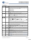
NWS
0
, NWS
1
Input-
Synchronous
Nibble Write Select 0, 1, Active LOW (CY7C1246V18 only). Sampled on the rising edge of
the K and K
clocks during write operations. Used to select which nibble is written into the device
during the current portion of the write operations. Nibbles not written remain unaltered.
NWS
0
controls D
[3:0]
and NWS
1
controls D
[7:4]
.
All the Nibble Write Selects are sampled on the same edge as the data. Deselecting a Nibble
Write Select ignores the corresponding nibble of data and not written into the device.
BWS
0
,
BWS
1
,
BWS
2
, BWS
3
Input-
Synchronous
Byte Write Select 0, 1, 2, and 3, Active LOW. Sampled on the rising edge of the K and K clocks
during write operations. Used to select which byte is written into the device during the current
portion of the write operations. Bytes not written remain unaltered.
CY7C1257V18 − BWS
0
controls D
[8:0]
CY7C1248V18 − BWS
0
controls D
[8:0]
and BWS
1
controls D
[17:9].
CY7C1250V18 − BWS
0
controls D
[8:0]
, BWS
1
controls D
[17:9]
, BWS
2
controls D
[26:18]
and BWS
3
controls D
[35:27]
.
All the Byte Write Selects are sampled on the same edge as the data. Deselecting a Byte Write
Select ignores the corresponding byte of data and not written into the device.
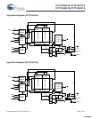
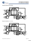
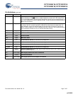
A Input-
Synchronous
Address Inputs. Sampled on the rising edge of the K clock during active read and write opera-
tions. These address inputs are multiplexed for both read and write operations. Internally, the
device is organized as 4M x 8 (2 arrays each of 2M x 8) for CY7C1246V18, 4M x 9 (2 arrays
each of 2M x 9) for CY7C1257V18, 2M x 18 (2 arrays each of 1M x 18) for CY7C1248V18, and
1M x 36 (2 arrays each of 512K x 36) for CY7C1250V18.
R/W
Input-
Synchronous
Synchronous Read/Write Input. When LD is LOW, this input designates the access type (read
when R/W
is HIGH, write when R/W is LOW) for loaded address. R/W must meet the setup and
hold times around edge of K.
QVLD Valid output
indicator
Valid Output Indicator. The Q Valid indicates valid output data. QVLD is edge aligned with CQ
and CQ
.
K Input-
Clock
Positive Input Clock Input. The rising edge of K is used to capture synchronous inputs to the
device and to drive out data through Q
[x:0]
when in single clock mode. All accesses are initiated
on the rising edge of K.
K Input-
Clock
Negative Input Clock Input. K is used to capture synchronous data being presented to the
device and to drive out data through Q
[x:0]
when in single clock mode.
CQ Clock Output Synchronous Echo Clock Outputs. This is a free running clock and is synchronized to the
input clock (K) of the DDR-II+. The timing for the echo clocks is shown in “Switching Character-
istics” on page 22.
CQ
Clock Output
Synchronous Echo Clock Outputs. This is a free running clock and is synchronized to the
input clock (K) of the DDR-II+. The timing for the echo clocks is shown in “Switching Character-
istics” on page 22.
[+] Feedback [+] Feedback