


CY7C1246V18, CY7C1257V18
CY7C1248V18, CY7C1250V18
Document Number: 001-06348 Rev. *D Page 13 of 27
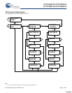
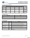
IDCODE
The IDCODE instruction loads a vendor-specific, 32-bit code into
the instruction register. It also places the instruction register
between the TDI and TDO pins and shifts the IDCODE out of the
device when the TAP controller enters the Shift-DR state. The
IDCODE instruction is loaded into the instruction register upon
power up or whenever the TAP controller is in a Test-Logic-Reset
state.
SAMPLE Z
The SAMPLE Z instruction connects the boundary scan register
between the TDI and TDO pins when the TAP controller is in a
Shift-DR state. The SAMPLE Z command puts the output bus
into a High-Z state until the next command is issued during the
Update-IR state.
SAMPLE/PRELOAD
SAMPLE/PRELOAD is a 1149.1 mandatory instruction. When
the SAMPLE/PRELOAD instructions are loaded into the
instruction register and the TAP controller is in the Capture-DR
state, a snapshot of data on the inputs and output pins is
captured in the boundary scan register.
Be aware that the TAP controller clock can only operate at a
frequency up to 20 MHz, while the SRAM clock operates more
than an order of magnitude faster. Because there is a large
difference in the clock frequencies, it is possible that during the
Capture-DR state, an input or output may undergo a transition.
The TAP may then try to capture a signal while in transition
(metastable state). This does not harm the device, but there is
no guarantee as to the value that is captured. Repeatable results
may not be possible.
To guarantee that the boundary scan register captures the
correct value of a signal, the SRAM signal must be stabilized
long enough to meet the TAP controller's capture setup plus hold
times (t
CS
and t
CH
). The SRAM clock input might not be captured
correctly if there is no way in a design to stop (or slow) the clock
during a SAMPLE/PRELOAD instruction. If this is an issue, it is
still possible to capture all other signals and simply ignore the
value of the CK and CK
captured in the boundary scan register.
After the data is captured, it is possible to shift out the data by
putting the TAP into the Shift-DR state. This places the boundary
scan register between the TDI and TDO pins.
PRELOAD places an initial data pattern at the latched parallel
outputs of the boundary scan register cells before the selection
of another boundary scan test operation.
The shifting of data for the SAMPLE and PRELOAD phases can
occur concurrently when required — that is, while data captured
is shifted out, the preloaded data can be shifted in.
BYPASS
When the BYPASS instruction is loaded in the instruction register
and the TAP is placed in a Shift-DR state, the bypass register is
placed between the TDI and TDO pins. The advantage of the
BYPASS instruction is that it shortens the boundary scan path
when multiple devices are connected together on a board.
EXTEST
The EXTEST instruction drives the preloaded data out through
the system output pins. This instruction also connects the
boundary scan register for serial access between the TDI and
TDO in the Shift-DR controller state.
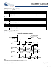
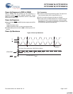
EXTEST Output Bus Tri-State
IEEE Standard 1149.1 mandates that the TAP controller be able
to put the output bus into a tri-state mode.
The boundary scan register has a special bit located at bit #108.
When this scan cell, called the “extest output bus tri-state,” is
latched into the preload register during the Update-DR state in
the TAP controller, it directly controls the state of the output
(Q-bus) pins, when the EXTEST is entered as the current
instruction. When HIGH, it enables the output buffers to drive the
output bus. When LOW, this bit places the output bus into a
High-Z condition.
This bit can be set by entering the SAMPLE/PRELOAD or
EXTEST command, and then shifting the desired bit into that cell,
during the Shift-DR state. During Update-DR, the value loaded
into that shift-register cell latches into the preload register. When
the EXTEST instruction is entered, this bit directly controls the
output Q-bus pins. Note that this bit is preset HIGH to enable the
output when the device is powered-up, and also when the TAP
controller is in the Test-Logic-Reset state.
Reserved
These instructions are not implemented but are reserved for
future use. Do not use these instructions.
[+] Feedback [+] Feedback