EVGA Corporation 2900 Saturn St. Suite B, Brea, CA 92821
Phone: 888 / 881-EVGA - 714 / 528-4500 - Fax: 714 / 528-4501
Page 36
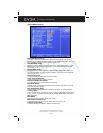
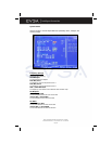
Memory Timings
Standard Memory Settings
Timing mode
Select automatic or manual set memory timing
tCL (CAS Latency)
CAS Latency (CAS# to read data valid)
tRCD
RAS# to CAS# delay for a RD/WR command to the same bank
tRP
Row Precharge time Precharge-to-Active or Auto-Refresh of the same bank
tRAS
Minimum RAS# active time
Command Per Clock (CMD)
Command timing setting (per clock unit)
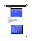
Advance Memory Settings
tRRD
RAS# to RAS# delay of different banks
AsyncLat
Max round trip latency from the CPU to the DRAM
tRC
RAS# to RAS# or auto refresh time of the same bank
tWR
Write recovery time
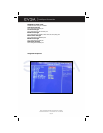
tRWT
Minimum read to write turnaround time
tWTR
Minimum write to read delay with same chip select
tREF
DRAM refresh rate
Read DQS Skew
Read DQS delayed with respect to the data. 1/96 MEMCLK per unit.
Read delay from Rx FIFO
Delay from DQS receiver enable to first data read from Rx FIFO.
Drive Strength Setting


