© 1999 National Semiconductor Corporation http://www.national.com
Printed in the U.S.A.
N
Section I. Introduction
The CLC3790093 Data Capture Board enables simple evaluation
of National Semiconductor’s High Speed Analog to Digital Con-
verters (ADCs) and the Diversity Receiver Chip Set (DRCS). The
Data Capture Board interfaces the outputs of these devices to the
standard serial port available on the back of most Personal
Computers (PCs). We have provided PC software to control the
data capture function and Matlab
®
scripts for data analysis.
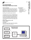
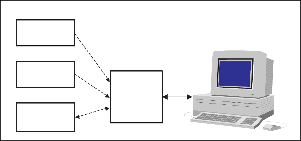
A block diagram of the evaluation test bed is shown below.
The Data Capture Board contains a field-programmable gate
array (FPGA) that controls its operation. An EPROM configures
the FPGA after power is applied. The serial interface is provided
by a UART (Universal Asynchronous Receiver/Transmitter), an
oscillator, and a level translator IC. The captured data is stored in
either three 32K x 8 static RAMs (organized into 24-bit words) or
in a FIFO containing 32K 18-bit words. LEDs provide a visual
indication of activity. DIP switches and a jumper configure several
capture functions.
Section II. Capturing Data from ADC
Evaluation Boards
Getting Started
To use the Data Capture board to capture data from a National
Semiconductor Analog to Digital converter, you will need the
following hardware, software, and documentation.
CLC-CAPT-PCASM
Data Capture Board User’s Guide
Table of Contents
I. Introduction
II. Capturing Data from ADC
Evaluation Boards
III. Capturing Data from the DRCS
Evaluation Boards
IV. Data Analysis using Matlab
Script Files
May 1999
Rev 1.0.0
CLC-CAPT-PCASM
Data Capture Board User’s Guide
CLC5956
Evaluation Board
CLC5958
Evaluation Board
Digital Receiver
ChipSet (DRCS)
Evaluation Board
Data
Capture
Board
National Semiconductor
High-Speed Converter
Evaluation Test Bed


