


http://www.national.com 10
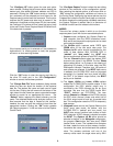
#4 & #5 as indicated in the Histogram Max Target
table. Due to a high data resolution and relatively
slow data rate, a relatively long period of time is
required for generating histogram data from the
DRCS with high decimation values in the DDC.
Under some circumstances, the serial PC interface
will time out. The program detects this condition and
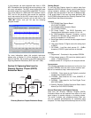
queries the user to continue. Click
“Yes”
to continue
and wait for the Progress Bar to run to completion.
Be patient, it could take several minutes depending
on the input amplitude and DDC decimation value
and Histogram Target Value. The last mode
description,
Debug Histogram
, provides further
description of the output file generated by the hard-
wired histogram generator.
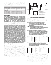
Histogram Target Table
3.
Capture Debug
mode configures the Capture
Board to collect data from the DRCS evaluation
board’s 20-bit parallel debug data bus. Because the
FIFO memory is limited to 18 bits, the user is given
the option to collect the full data width in the SRAM
by selecting the
20 Bits
menu button. As previously
mentioned, parallel data which runs at the full clock
speed (i.e.
Mixer Out
at Debug port) gets deci-
mated by 6 due to the fact that the FPGA requires
multiple clock strobes to address and write data into
the SRAM. Choosing the
Upper 18 Bits
option will
use the high speed FIFO for the memory element
and collect a contiguous 32K block of data. The
Debug
data port provides users access to nodes
internal to the CLC5902 DDC. Refer to the DRCS
Evaluation Board User Manual and CLC5902 data
sheet for more detailed information.
4.
Histogram Debug
mode configures the Capture
Board to generate a histogram file using the parallel
data as the source. The hardware requires multiple
clock strobes to increment each SRAM value. Even
though the data used is not a contiguous block, the
probability density information is retained. The
SRAM depth (32K) is used to store the data bin
values; therefore, the histogram generator is limited
to 15-bits of resolution (there are only 32,767 bins).
The values of all 32K bins will be read out of the
SRAM and sent out to the users PC regardless of
the resolution of the data source. The DRCS
Debug
data will be displayed at the 15-bit resolution limit
(this is also the case for the DRCS 24-bit Serial Out
data) and the histogram will be centered about
16,384 assuming there is no intentional DC offset.
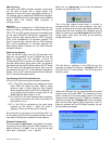
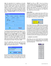
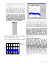
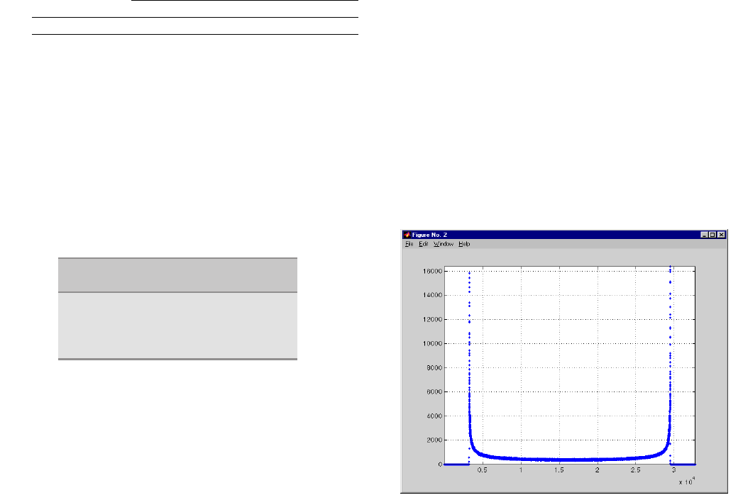
The following figure displays the sine wave histo-
gram data of the DRCS output generated by the
Capture Board at an input frequency of 150MHz and
16dBm in amplitude using all the default DRCS set-
tings. The data source was the DDC serial output
(
Capture Histogram
mode was used where
Fsample is 270KHz) and therefore took several
minutes to collect. In this scenario the 24-bit data
source resolution is truncated to the 15-bits (32K) of
available SRAM. The histogram peak target was set
to 16K which required over 16 million data points be
processed for the input level of -2dB below full scale.
The number of data points is proportional to the Max
Target and the amplitude range of the data (the X-
axis). The “Plot Data” menu function of the analysis
tools was used to generate the actual Matlab plot figure.
DRCS Evaluation Setup Sanity Check
The following discussion is to confirm the DRCS
evaluation setup. The example uses a Fourier analysis of
a simple, single tone, sinusoidal IF input to the DRCS. It
is assumed that Setup.exe on the evaluation kit’s
CDROM has installed the necessary files in the user’s
PC and the DRCS and Data Capture hardware is config-
ured as shown in the diagram at the front of
Section III
. It
is also assumed that Matlab (version 5.1 or higher) is
available. Reconfiguration of the DRCS through its Con-
trol Panel software is not required for these two tests. The
DRCS default values contained within the micro-control-
ler with SW2:1-8 = OFF (on DRCS board) will configure
the CLC5902 with the proper values. If the power has
been applied while in another state or if the user has
RESET
the micro-controller with a different switch set-
ting, then set the SW2 switches to OFF and press the
RESET
button on the DRCS Evaluation board.
**
Apply an IF input signal
to the AIN1 jack on the
DRCS Evaluation board at 150MHz and 0dBm. The
DDC mixer is set to -5.97MHz which brings the
aliased (Fclk ADC = 52MHz; 3rd alias = 156MHz)
signal down to +30KHz. The DDC then filters and
decimates the data and sends it out the serial port
(
AOUT
) in the “packed”, “muxed_mode” format.
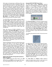
SW1; #4 SW1; #5
Histogram
Target Value
0 0 16K
0 1 8K
1 0 4K
1 1 2K