


http://www.national.com
8
24-bit words via the serial port as 96K bytes. Each word
is interpreted as a 24-bit two’s complement integer and
stored as 32K ASCII words in a user defined file. Each
value is terminated with a carriage return (hexadecimal
0D). When a Diversity Receiver Evaluation Board is
attached to the Data Capture Board, data narrower than
24 bits is aligned to the most significant bit with unused
lower bits set to 0s. Serial data is always 24-bits wide.
Because of the various DRCS data output formats, care
must be exercised to ensure that configuration conflicts
do not occur between the Data Capture board and the
DRCS board. Such conflicts usually lead to unpredictable
data formats. The default DRCS settings,
“I/Q_Packed,
Mux_Mode”,
are compatible with the Data Capture
Board’s 24-bit serial and 16-bit parallel formats.
The “CLK” SMA connector provides a buffered output of
the DRCS Serial Clock (SCLK) divided by 2. The
CLC5902
“RATE”
register can be used to further divide
this clock. This clock output is intended for phase locking
a signal source to the DRCS XTAL oscillator. Because of
the FPGA speed limitations, DRCS Serial Clock “RATE”
settings <2 are not recommended. The default DRCS
settings and XTAL oscillator yield a 13MHz output from
this SMA jack.
Serial data from the CLC5902 (DDC/AGC) can be
configured for
“I/Q_Packed, Mux_Mode”
in the majority
of evaluations (refer to the CLC5902 data sheet or the
DRCS Evaluation Board User Manual). For proper opera-
tion, a decimation of at least 192 in the DDC is required
to complete the transfer of the whole 96-bit word (24-bits
each of CHA I & Q phase and CHB I & Q phase). The
Data Capture board de-serializes the DRCS data stream,
registers the selected channel and phase, stores the data
in SRAM, then reads and formats the SRAM data to a
24-bit word for transmission to the PC via its serial
communications port.
Parallel and Debug port data can be written directly to the
18-bit by 32K FIFO or to the 24-bit by 32K SRAM.
Because the FIFO has its own address counter, it is
capable of contiguous block capture up to 75MSPS and
is the recommended means of data capture for Fourier
Analysis of high speed data. The SRAM address and
write is controlled by the FPGA, which requires about 6
clock strobes per write cycle resulting in data decimation.
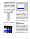
The SRAM is useful for displaying time records of data or
collecting contiguous blocks of slower data that have
been decimated by the CLC5902 DDC. The SRAM is
the memory element used for the board’s hardwired
histogram data generation.
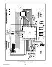
Capture Board Hardware Configuration Options for
DRCS data capture
Place the
WCLK
(FIFO write clock) jumper in the
“PIN
120”
position, the
VCORE
should be in the
“5V”
position
and the eight
SW1
switches in their
“OFF”
position.
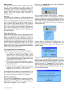
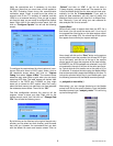
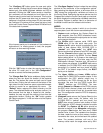
Using the DATA CAPTURE Control Panel
The Data Capture Program,
“capture.exe”
, must be
copied into a directory on the user’s PC. The setup/install
program on the CDROM automatically places this
program in a default directory (c:\nsc\). The program
generates a user *.ini file within this same directory.
The file is used to store the user options and is updated
each time the user changes the options and runs the
program. When the Data Capture Program is started, a
graphical user interface (GUI) Control Panel is placed on
the PC desktop.
The
left mouse button
can be used to drag the control
panel to the desired position on the desktop. The Data
Capture control panel should not be placed on top of the
Windows task bar, otherwise the software may behave
erratically. A left click on the
?
button will open an informa-
tional text file. The program configuration variables must
be setup prior to running the program using the
“Start”
button. Clicking the
right mouse button
within the con-
trol panel brings up the user configuration options menu.
The left mouse button is again used to select the desired
menu option.
The following discusses the function of the various menu
options:
The
“Exit”
button terminates the Data Capture Program.
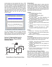
The
“About”
button opens a window that displays the
version of the Data Capture Program as well as the
firmware revision of the FPGA on the Data Capture
Board. Clicking the left mouse button on the
“SysInfo”
button in the About window replaces it with the System
Information window that displays some details about your
PC. Clicking the left mouse button on the
“OK”
button in
the System Information window closes it and returns you
to the About window. Clicking the left mouse button on
the
“Visit our web page”
text will open National Semi-
conductor’s web page using your internet browser.
Clicking the left mouse button on the
“OK”
button in the
“About”
window will close it.
The
“Auto Hide”
and
“Always on Top”
selections
enable and disable these functions. A check mark to the
left of each selection indicates when it is enabled.