


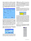
3
http://www.national.com
complement number can be converted to offset binary by
inverting the MSB. This is the first step in the Matlab
routine for FFT analysis.
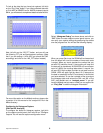
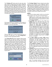
Histogram Mode
In the second mode of operation, the “Histogram” mode,
the data capture board operates as a hardware histo-
grammer. The board does not collect a contiguous record
from the ADC; instead, it compiles statistical information
by counting the number of times that the ADC
outputs each code. The most significant 15 bits of the
converter define 32K histogram bins. The MSB of the
data is inverted before being stored (all data is treated as
offset binary format). ADC data is aligned to the least sig-
nificant bit, and unused higher bits are set to 0s. Each bin
is cleared initially. The ADC output code is used as the
address for the SRAM on the board, and as each code is
read by the Data Capture board, the data at that location
in the SRAM is read, incremented and written back to the
SRAM. This counting requires multiple clock cycles, so
the data is not counted in real time. In fact, 11 samples of
data are missed for each sample that is counted. The his-
togram capture terminates when a bin reaches the count
specified by DIP switches 4 and 5. The 32K histogram bin
counts are then returned via the serial port. If the input
signal to the ADC is a pure sinusoid, then the histogram
information can be compared to the theoretical
probability density of a sinusoid and the linearity of the
ADC can be calculated. The supplied Matlab script
DNL_INL uses this method. Please refer to the IEEE
Standard for Digitizing Waveform Recorders (IEEE Std
1057-1994) for more information about this technique.
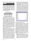
Hardware Configuration
Jumpers
The data capture board has 3 jumpers that must be con-
figured before use. The first jumper, VCORE, sets the
core voltage used by the FPGA. This jumper is always set
to 5V. (A voltage regulator on the board reduces the sup-
plied +5V to +3.3V for the FPGA I/O and other
components on the board.) The second jumper, WCLK,
selects the clock source for the FIFO. When capturing
data from an ADC evaluation board,
WCLK should
always be set to RDY2
. This selects the DR (Data
Ready) clock line from the ADC evaluation board pin
20B. The third jumper block, J2, is unused.
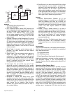
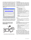
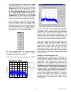
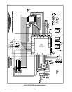
Data Capture Board Block Diagram
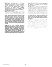
DIP Switches
Five of the eight DIP switches are used to configure
several capture functions as follows.
DIP switch 1:
This DIP switch specifies whether a
Diversity Receiver Evaluation Board or an
ADC Evaluation Board is attached to the Data
Capture Board.
ON
→
ADC Evaluation Board is attached.
Captured data is aligned to the least significant
bit with unused higher bits set to 0s.
DIP switches 2 and 3:
When DIP switch 1 is ON to
indicate that an ADC Evaluation Board is attached,
DIP switches 2 and 3 specify the width of the ADC
data so it can be aligned to the least significant bit
and unused higher bits can be set to 0s.
DIP switches 4 and 5:
These DIP switches specify the
maximum histogram bin count. The histogram
capture terminates when any bin reaches the count
specified by these switches.
A maximum count of 16384 corresponds to approxi-
mately 2.5 million total samples for a 12-Bit ADC. The
capture is very fast (on the order of 1 second for a 52
MSPS clock rate) so there is not much advantage in set-
ting the switches for a lower maximum count. The other
settings are more useful for the DRCS evaluations
because the effective clock rate can become very low
with certain output formats and decimation ratios.
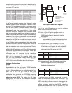
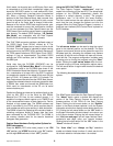
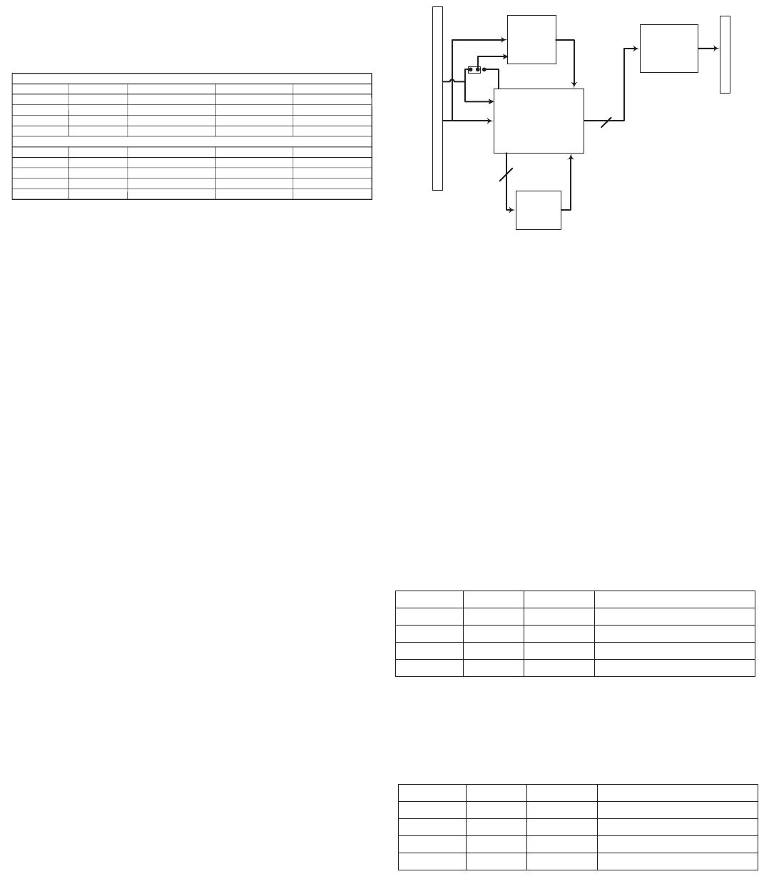
CLC5956 Data
Analog Input Condition Offset Binary Number Two's Complement ASCII Value Stored
Ain- >> Ain - Full Scale 0000 0000 0000 1000 0000 0000 2048
Ain- > Ain - Mid Scale 0111 1111 1111 1111 1111 1111 4095
Ain > Ain- + Mid Scale 1000 0000 0000 0000 0000 0000 0
Ain >> Ain- + Full Scale 1111 1111 1111 1111 1111 1111 2047
CLC5958 Data
Analog Input Condition Offset Binary Number Two's Complement ASCII Value Stored
Ain- >> Ain - Full Scale 00 0000 0000 0000 10 0000 0000 0000 8192
Ain- > Ain - Mid Scale 01 0111 1111 1111 11 1111 1111 1111 16383
Ain > Ain- + Mid Scale 10 0000 0000 0000 00 0000 0000 0000 0
Ain >> Ain- + Full Scale 11 1111 1111 1111 01 1111 1111 1111 8191
FPGA Performs:
State Machine
Signal Format Conversion
Data Routing
Data
12-18
Bits
J1
Eurocard
Connector
FPGA
SRAM
24-bits
32k depth
FIFO
18-bits
32k depth
UART
J9
9-pin
Serial Cable
Connector
24
Serialized
Data Stream
Note: Primary data path shown.
Control lines not shown
RDY2
WCLK
Clock
Switch: 2 3 Number of Bits in ADC
OFF OFF 18
OFF ON 16
ON OFF 14
ON ON 12
Switch: 4 5 Maximum Count
OFF OFF 16384
OFF ON 8192
ON OFF 4096
ON ON 2048