


© Copyright IBM Corp. 2004. All rights reserved. 19
Chapter 2. Architecture and technical
overview
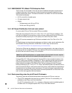
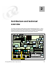
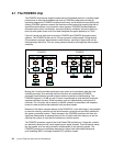
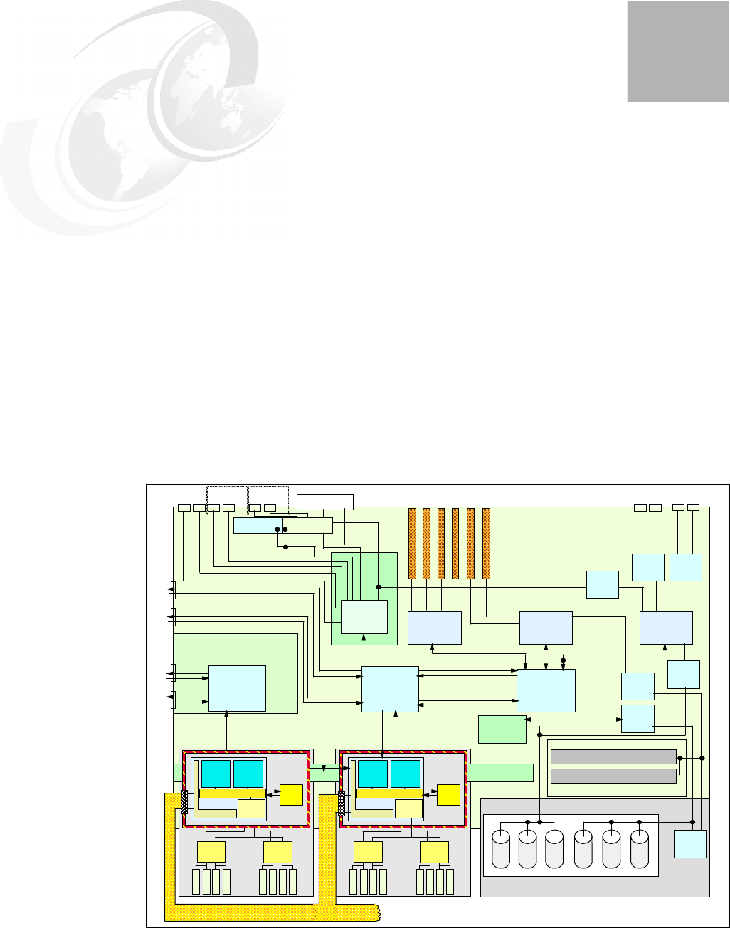
This chapter discusses the overall system architecture represented by Figure 2-1, with its
major components described in the following sections. The bandwidths that are provided
throughout the section are theoretical maximums used for reference. You should always
obtain real-world performance measurements using production workloads.
Figure 2-1 p5-570 logic data flow
2
D
I
M
M
D
I
M
M
D
I
M
M
D
I
M
M
SMI-II SMI-II
D
I
M
M
D
I
M
M
D
I
M
M
D
I
M
M
shared L2 cache
distributed switch
core
core
L3
cache
DCM
D
I
M
M
D
I
M
M
D
I
M
M
D
I
M
M
SMI-II SMI-II
D
I
M
M
D
I
M
M
D
I
M
M
D
I
M
M
memory
controller
Vertical Fabric
bus
2 (Proc Clk):1
8 Bytes each dir
Elastic Intfc
SMP flex interconnect cable (SMP Fabric bus)
2 (Proc Clk):1
8 Bytes each dir
Elastic Intfc
Enterprise
RIO HUB
Enterprise
RIO HUB
RIO-2 expansion
card
RIO-2 bus
2 B (Diff'l) each dir
1 GB/sec
GX+ bus
3 (Proc Clk):1
4 Bytes each dir
Elastic Intfc
GX+ bus
3 (Proc Clk):1
4 Bytes each dir
Elastic Intfc
RIO-2 bus
2 B (Diff'l) each dir
1 GB/sec
PCI-X Host
bridge
RIO-2 bus
2 B (Diff'l) each dir
1 GB/sec
PCI-X to PCI-X
bridge 2
PCI-X to PCI-X
bridge 0
PCI-X to PCI-X
bridge 1
PCI-X slot #6 #5 #4 #3 #2 #1
133 MHz
optional media backplane
slim-line media device
slim-line media device
Dual SCSI
Ultra320
IDE
controller
FSP
operator panel
interface card
133 MHz
66 MHz
133 MHz
133 MHz
SCSI-IDE
conv
RAID
enablement
card
Two Eth
ports
Dual 1 GB
Ethernet
USB
Two USB
ports
Dual SCSI
Ultra320
CUoD key card
Serial
Two HMC
Eth ports
Two SPCN
ports
6-pack disk drive backplane
shared L2 cache
memory
controller
distributed switch
core
core
L3
cache
DCM
POWER5 POWER5
Two serial
ports