


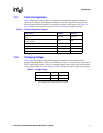

21555 PCI-to-PCI Bridge Evaluation Board User’s Guide 11
Introduction
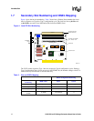
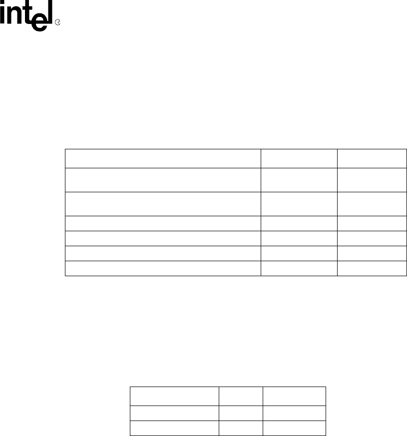
1.6.1 Clock Configuration
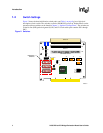
Table 3 describes the resistor jumpers to install that connect p_clk and s_clk_o to the Mictor
connectors. To improve signal integrity and minimize noise, these signals are not wired to the
Mictor connectors. Resistor jumpers also control the selection of clock signals. See Figure 3 on
page 10 for the resistor jumper locations. See Table A-3 on page 24 for Mictor pinouts.
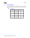
1.6.2 Clamping Voltage
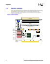
Table 4 gives the clamping voltage resistor jumper configurations. These jumper resistors
designate the DE1B55503 as a 3.3V or a 5V PCI device. A mix of 3.3 and 5 V cards is not allowed.
The E1 regulator provides the 3.3V or 5 V clamping voltage for the local bus. The resistor jumpers
connect s_vio to either 3.3V or 5V. Figure 4 on page 12 shows the location of the resistor jumpers.
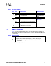
Table 3. Clock Configuration Jumpers
Clock Source Installed Removed
Use the s_clk_o signal from the 21555 as the local
clock.
R65, R73 R68, R93
Use the s_clk_i that is the output of the clock buffer
as the local clock.
R73 R68
Use the system slot to drive the 21555 s_clk_i. R68 R73
Use an oscillator as the asynchronous local clock. R93 R65, R68
Use the system slot to provide the local clock. R92, R116, R69 R91, R115, R72
Use the clock buffer to provide the local clock. R91, R115, R72 R92, R116, R69
Table 4. Voltage Clamp
a
a. Only one jumper resistor (R95 or R97) may be installed at
a time. Installing both or no jumper resistors is not allowed.
Function Installed Removed
s_vio is 3.3V R95 R97
s_vio is 5V R97 R95