


21555 PCI-to-PCI Bridge Evaluation Board User’s Guide 7
Introduction
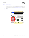
Note: See Table A-2 on page 24 for Mictor pinouts.
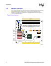
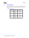
1.3.2 Switches and Jumper
The DE1B55503 uses a combination of DIP switch, stake-pin and zero ohm resistor jumpers to
control the various configuration options. See Section 1.4, Section 1.5, and Section 1.6 for
information.
• J8 is a single stake pin jumper. See Section 1.5 for information.
• J9, J20, and J21 are five-switch switch packs. The dual-pole switches are labeled SW1 through
SW5. They control the options at power up such as the direction of the REQ# and GNT# lines,
the on-board parallel ROM functions, and the enabling of the asynchronous clock options for
the local bus. See Section 1.4 for information.
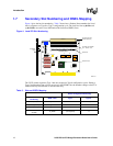
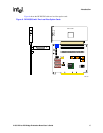
• Figure 3 on page 10 identifies the location of each configuration jumper.
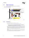
1.3.3 Devices
• E1 is the voltage regulator that produces the 3.3 and 5 V clamping signal. See Section 1.6.2.
• E2 is the 21555 PCI-to-PCI Bridge.
• E3 is the clock buffer.
• E4 is the serial ROM (SROM).
• Y1 is a 33.333 MHz crystal oscillator that can be used for an independent local clock signal.
• E5 is the Parallel ROM. This device is nonvolatile EEPROM. See Section 2.3.2,
“Programming the Flash ROM” on page 18.
• E7, E8, and E9 are address latches.
• E6 (not shown) is the empty socket for attaching a ROM emulator.
• L1 is a LED that indicates the status of the LOO bit (LED On or Off bit) which is switched
through software. This LED can light if jumper J8 is installed.
• L2 is a LED that indicates DE1B55503 5Vdc power status.